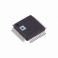
AD7484BSTZ Analog Devices Inc, AD7484BSTZ Datasheet - Page 16

AD7484BSTZ
Manufacturer Part Number
AD7484BSTZ
Description
IC ADC 14BIT SAR 3MSPS 48-LQFP
Manufacturer
Analog Devices Inc
Datasheet
1.AD7484BSTZ.pdf
(20 pages)
Specifications of AD7484BSTZ
Data Interface
Parallel
Number Of Bits
14
Sampling Rate (per Second)
3M
Number Of Converters
1
Power Dissipation (max)
90mW
Voltage Supply Source
Analog and Digital
Operating Temperature
-40°C ~ 85°C
Mounting Type
Surface Mount
Package / Case
48-LQFP
Resolution (bits)
14bit
Sampling Rate
3MSPS
Input Channel Type
Single Ended
Supply Voltage Range - Analog
4.75V To 5.25V
Supply Voltage Range - Digital
4.75V To 5.25V
Lead Free Status / RoHS Status
Lead free / RoHS Compliant
For Use With
EVAL-AD7484CBZ - BOARD EVALUATION FOR AD7484
Lead Free Status / RoHS Status
Lead free / RoHS Compliant, Lead free / RoHS Compliant
Available stocks
Company
Part Number
Manufacturer
Quantity
Price
Company:
Part Number:
AD7484BSTZ
Manufacturer:
ADI30
Quantity:
221
Company:
Part Number:
AD7484BSTZ
Manufacturer:
Analog Devices Inc
Quantity:
10 000
Part Number:
AD7484BSTZ
Manufacturer:
ADI/亚德诺
Quantity:
20 000
AD7484
The maximum slew rate at the input of the ADC should be
limited to 500 V/µS while BUSY is low to avoid corrupting the
ongoing conversion. In any multiplexed application where the
channel is switched during conversion, this should happen as
early as possible after the BUSY falling edge.
Reading Data from the AD7484
Data is read from the part via a 15-bit parallel data bus with
the standard CS and RD signals. The CS and RD signals are
internally gated to enable the conversion result onto the data
bus. The data lines D0 to D14 leave their high impedance
state when both CS and RD are logic low. Therefore, CS
may be permanently tied logic low if required, and the RD
signal used to access the conversion result. Figure 29 shows a
timing specification called t
that should be left after any data bus activity before the next
conversion is initiated.
Writing to the AD7484
The AD7484 features a user-accessible offset register. This
allows the bottom of the transfer function to be shifted by
±200 mV. This feature is explained in more detail in the
Offset/Overrange section.
To write to the offset register, a 15-bit word is written to the
AD7484 with the 12 LSBs containing the offset value in twos
complement format. The 3 MSBs must be set to 0. The offset
value must be within the range −1310 to +1310, corresponding
to an offset from −200 mV to +200 mV. The value written to the
offset register is stored and used until power is removed from
the device, or the device is reset. The value stored may be
updated at any time between conversions by another write to
the device. Table 8 shows some examples of offset register values
and their effective offset voltage. Figure 30 shows a timing
diagram for writing to the AD7484.
Table 8. Offset Register Examples
Code
(Dec)
−1310
−512
+256
+1310
Driving the CONVST Pin
To achieve the specified performance from the AD7484, the
CONVST pin must be driven from a low-jitter source. Since the
falling edge on the CONVST pin determines the sampling
instant, any jitter that may exist on this edge will appear as noise
when the analog input signal contains high frequency
components. The relationship between the analog input
frequency (f
the equation
IN
D14 to
D12
000
000
000
000
), timing jitter (t
D11 to D0 (Twos
Complement)
1010 1110 0010
1110 0000 0000
0001 0000 0000
0101 0001 1110
QUIET
j
), and resulting SNR is given by
. This is the amount of time
Offset
(mV)
−200
−78.12
+39.06
+200
Rev. A | Page 16 of 20
4.75V TO 5.25V
As an example, if the desired SNR due to jitter was 100 dB
with a maximum full-scale analog input frequency of
1.5 MHz, ignoring all other noise sources, the result is an
allowable jitter on the CONVST falling edge of 1.06 ps. For a
14-bit converter (ideal SNR = 86.04 dB), the allowable jitter will
be greater than the figure given above, but due consideration
must be given to the design of the CONVST circuitry to achieve
14-bit performance with large analog input frequencies.
Typical Connection
Figure 23 shows a typical connection diagram for the AD7484
operating in Parallel Mode 1. Conversion is initiated by a falling
edge on CONVST . Once CONVST goes low, the BUSY signal
goes low, and at the end of conversion, the rising edge of BUSY
is used to activate an interrupt service routine. The CS and RD
lines are then activated to read the 14 data bits (15 bits if using
the overrange feature).
In Figure 23, the V
logic output levels being either 0 V or DV
to V
For example, if DV
3 V supply, the logic output levels would be either 0 V or 3 V.
This feature allows the AD7484 to interface to 3 V devices while
still enabling the ADC to process signals at a 5 V supply.
DIGITAL
SUPPLY
ADM809
µC/µP
DRIVE
SNR
controls the voltage value of the output logic signals.
0.1 µ F
10 µ µ F
JITTER
PARALLEL
INTERFACE
+
( )
dB
Figure 23. Typical Connection Diagram
DRIVE
DD
1nF
=
10
is supplied by a 5 V supply and V
pin is tied to DV
RESET
MODE1
MODE2
WRITE
CLIP
NAP
STBY
D0 TO D13
CS
CONVST
RD
BUSY
V
log
DRIVE
0.1 µ F
(
AD7484
2
π
DV
×
DD
f
IN
REFOUT
1
REFSEL
AV
REFIN
C
×
DD
BIAS
VIN
t
j
)
DD
0.1 µ F
2
DD
, which results in
. The voltage applied
0.47 µ F
0.47 µ F
0V TO 2.5V
1nF
+
4.75V TO 5.25V
47 µ F
ANALOG
REFERENCE
SUPPLY
AD780 2.5V
DRIVE
by a


