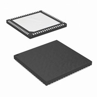
KAD2710L-10Q68 Intersil, KAD2710L-10Q68 Datasheet - Page 13

KAD2710L-10Q68
Manufacturer Part Number
KAD2710L-10Q68
Description
IC ADC 10BIT 105MSPS SGL 68-QFN
Manufacturer
Intersil
Series
FemtoCharge™r
Datasheet
1.KAD2710L-17Q68.pdf
(16 pages)
Specifications of KAD2710L-10Q68
Number Of Bits
10
Sampling Rate (per Second)
105M
Data Interface
Parallel
Number Of Converters
1
Power Dissipation (max)
202mW
Voltage Supply Source
Single Supply
Operating Temperature
-40°C ~ 85°C
Mounting Type
Surface Mount
Package / Case
68-VQFN Exposed Pad, 68-HVQFN, 68-SQFN, 68-DHVQFN
For Use With
KDC2710LEVAL - DAUGHTER CARD FOR KAD2710
Lead Free Status / RoHS Status
Lead free / RoHS Compliant
Analog
Analog
A back-to-back transformer scheme is used to improve
common-mode rejection, which keeps the common-mode
level of the input matched to V
resistor should be determined based on the desired load
impedance.
The sample and hold circuit design uses a switched
capacitor input stage, which creates current spikes when the
sampling capacitance is reconnected to the input voltage.
This creates a disturbance at the input which must settle
before the next sampling point. Lower source impedance will
result in faster settling and improved performance. Therefore
a 1:1 transformer and low shunt resistance are
recommended for optimal performance.
A differential amplifier can be used in applications that
require dc coupling. In this configuration the amplifier will
typically determine the achievable SNR and distortion. A
typical differential amplifier circuit is shown in Figure 25.
Clock Input
The sample clock input circuit is a differential pair (see
Figure 29). Driving these inputs with a high level (up to
1.8V
lowest jitter performance.
Input
Analog
Input
FIGURE 23. TRANSFORMER INPUT, GENERAL APPLICATION
FIGURE 24. TRANSFORMER INPUT FOR HIGH IF
In
49.9O
PP
1000pF
1000pF
Ω
0.01µF
FIGURE 25. DIFFERENTIAL AMPLIFIER INPUT
on each input) sine or square wave will provide the
0.22µF
69.8O
ADT1-1WT
APPLICATIONS
ADTL1-12
Ω
69.8O
100O
100O
Ω
Ω
Ω
ADTL1-12
ADT1-1WT
348O
348O
CM
13
Ω
Ω
CM
. The value of the shunt
0.1µF
25O
0.1µF
25O
25O
25O
Ω
Ω
Ω
Ω
50O
217O
Ω
0.1µF
Ω
KAD2710L
VCM
KAD2710L
VCM
KAD2710
VCM
KAD2710L
The recommended drive circuit is shown in Figure 26. The
clock can be driven single-ended, but this will reduce the
edge rate and may impact SNR performance.
Clock
Use of the clock divider is optional. The KAD2710L's ADC
requires a clock with 50% duty cycle for optimum
performance. If such a clock is not available, one option is to
generate twice the desired sampling rate and use the
KAD2710L's divide-by-2 setting. This frequency divider uses
the rising edge of the clock, so 50% clock duty cycle is
assured. Table 2 describes the CLKDIV connection.
CLKDIV is internally pulled low, so a pull-up resistor or logic
driver must be connected for undivided clock.
Jitter
In a sampled data system, clock jitter directly impacts the
achievable SNR performance. The theoretical relationship
between clock jitter (t
is illustrated in Figure 27.
Where t
Input
SNR
AVDD2
10 0
9 5
9 0
8 5
8 0
7 5
7 0
6 5
6 0
5 5
5 0
1
=
20 log
J
FIGURE 26. RECOMMENDED CLOCK DRIVE
CLKDIV PIN
is the RMS uncertainty in the sampling instant.
1nF
AVDD
AVSS
FIGURE 27. SNR vs CLOCK JITTER
10
tj=1 00p s
1kO
TABLE 2. CLKDIV PIN SETTINGS
TC4-1W
⎛
⎝
Ω
------------------- -
2πf
1
IN
J
t
) and SNR is shown in Equation 1 and
J
10
⎞
⎠
Input Frequency - MHz
tj=1 0p s
1nF
1kO
Ω
tj=1 ps
tj=0.1p s
DIVIDE RATIO
100
200O
2
1
December 5, 2008
Ω
FN6818.0
(EQ. 1)
1 4 Bits
1 2 Bits
10 Bits
CLKP
CLKN
10 00


