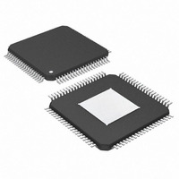
MAX105ECS+ Maxim Integrated Products, MAX105ECS+ Datasheet - Page 19

MAX105ECS+
Manufacturer Part Number
MAX105ECS+
Description
IC ADC 6BIT 800MSPS DL 80TQFP
Manufacturer
Maxim Integrated Products
Datasheet
1.MAX105ECS.pdf
(21 pages)
Specifications of MAX105ECS+
Number Of Bits
6
Sampling Rate (per Second)
800M
Data Interface
Parallel
Number Of Converters
2
Power Dissipation (max)
2.6W
Voltage Supply Source
Analog and Digital
Operating Temperature
-40°C ~ 85°C
Mounting Type
Surface Mount
Package / Case
80-TQFP Exposed Pad, 80-eTQFP, 80-HTQFP, 80-VQFP
Number Of Adc Inputs
2
Conversion Rate
800 MSPs
Resolution
6 bit
Snr
37 dB
Voltage Reference
2.5 V
Supply Voltage (max)
3.6 V
Supply Voltage (min)
3 V
Maximum Power Dissipation
3.5 W
Maximum Operating Temperature
+ 85 C
Mounting Style
SMD/SMT
Input Voltage
3.3 V
Minimum Operating Temperature
- 40 C
Lead Free Status / RoHS Status
Lead free / RoHS Compliant
Figure 11. Aperture Timing
clock design limits aperture jitter to typically 1.5ps
Figure 11 depicts the aperture jitter (t
sample-to-sample variation in the aperture delay.
Aperture delay (t
rising edge of the sampling clock and the instant when
an actual sample is taken
For a waveform perfectly reconstructed from digital
samples, the theoretical maximum SNR is the ratio of
the full-scale analog input (RMS value) to the RMS
quantization error (residual error). The ideal, theoretical
minimum analog-to-digital noise is caused by quantiza-
tion error only and results directly from the ADC’s reso-
lution (N-Bits):
In reality, there are other noise sources besides quanti-
zation noise: thermal noise, reference noise, clock jitter
(see Aperture Uncertainties). SNR is computed by tak-
ing the ratio of the RMS signal to the RMS noise, which
includes all spectral components minus the fundamen-
tal, the first four harmonics, and the DC offset.
SINAD is computed by taking the ratio of the RMS sig-
nal to all spectral components minus the fundamental
and the DC offset.
ENOB specifies the dynamic performance of an ADC at
a specific input frequency, amplitude, and sampling
rate relative to an ideal ADC’s quantization noise. For a
full-scale input ENOB is computed from:
SAMPLING
Signal-to-Noise Plus Distortion (SINAD)
INSTANT
ANALOG
INPUT
CLK+
CLK-
SNR
ENOB = (SINAD - 1.76
t
AD
Effective Number of Bits (ENOB)
MAX[dB]
AD
______________________________________________________________________________________
Signal-to-Noise Ratio (SNR)
Dual, 6-Bit, 800Msps ADC with On-Chip,
) is the time defined between the
= 6.02
t
t
AW
(Figure 11).
AJ
dB
t
t
t
AW
AJ
AD
: APERTURE JITTER
: APERTURE DELAY
: APERTURE WIDTH
x N + 1.76
dB
) / 6.02
AJ
), which is the
MAX105
dB
dB
RMS
Wideband Input Amplifier
.
THD is typically the ratio of the RMS sum of the first four
harmonics of the input signal to the fundamental itself.
This is expressed as:
where V1 is the fundamental amplitude, and V
V
monics.
SFDR is the ratio expressed in decibels of the RMS
amplitude of the fundamental to the RMS value of the
next largest spurious component, excluding DC offset.
The two-tone IMD is the ratio expressed in decibels of
either input tone to the worst 3rd-order (or higher) inter-
modulation products. The individual input tone levels
are at -7dB full-scale and their envelope peaks at -1dB
full-scale.
TRANSISTOR COUNT: 12,286
5
are the amplitudes of the 2nd- through 5th-order har-
THD
Spurious-Free Dynamic Range (SFDR)
=
20
Total Harmonic Distortion (THD)
x
log (
Two-Tone Intermodulation
V
2
2
+
Chip Information
V
3
2
+
V
Distortion (IMD)
4
2
+
V
5
2
) /
V
1
2
2
through
)
19


