MAX105ECS+ Maxim Integrated Products, MAX105ECS+ Datasheet - Page 2
MAX105ECS+
Manufacturer Part Number
MAX105ECS+
Description
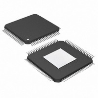
IC ADC 6BIT 800MSPS DL 80TQFP
Manufacturer
Maxim Integrated Products
Datasheet
1.MAX105ECS.pdf
(21 pages)
Specifications of MAX105ECS+
Number Of Bits
6
Sampling Rate (per Second)
800M
Data Interface
Parallel
Number Of Converters
2
Power Dissipation (max)
2.6W
Voltage Supply Source
Analog and Digital
Operating Temperature
-40°C ~ 85°C
Mounting Type
Surface Mount
Package / Case
80-TQFP Exposed Pad, 80-eTQFP, 80-HTQFP, 80-VQFP
Number Of Adc Inputs
2
Conversion Rate
800 MSPs
Resolution
6 bit
Snr
37 dB
Voltage Reference
2.5 V
Supply Voltage (max)
3.6 V
Supply Voltage (min)
3 V
Maximum Power Dissipation
3.5 W
Maximum Operating Temperature
+ 85 C
Mounting Style
SMD/SMT
Input Voltage
3.3 V
Minimum Operating Temperature
- 40 C
Lead Free Status / RoHS Status
Lead free / RoHS Compliant


ABSOLUTE MAXIMUM RATINGS
AV
OV
AGND to OGND ................................................... -0.3V to +0.3V
P0I± to P5I± and A0I± to A5I±
P0Q± to P5Q±, A0Q± to A5Q±
REF to AGNDR...........................................-0.3V to AV
Differential Voltage Between INI+ and INI- ....................-2V, +2V
Differential Voltage Between INQ+ and INQ-.................-2V, +2V
Dual, 6-Bit, 800Msps ADC with On-Chip,
Wideband Input Amplifier
Stresses beyond those listed under “Absolute Maximum Ratings” may cause permanent damage to the device. These are stress ratings only, and functional
operation of the device at these or any other conditions beyond those indicated in the operational sections of the specifications is not implied. Exposure to
absolute maximum rating conditions for extended periods may affect device reliability.
ELECTRICAL CHARACTERISTICS
(AV
= 0, f
otherwise noted. Typical values are at T
2
DC ACCURACY
Resolution
Integral Nonlinearity (Note 1)
Differential Nonlinearity
(Note 1)
Offset Voltage
O ffset M atchi ng Betw een AD C s
ANALOG INPUTS (INI+, INI-, INQ+, INQ-)
Input Open-Circuit Voltage
Input Open-Circuit Voltage
Matching
Common Mode Input Voltage
Range (Note 3)
Full-Scale Analog Input
Voltage Range (Note 4)
Input Resistance
Input Capacitance
Input Resistance Temperature
Coefficient
Full-Power Analog Input BW
REFERENCE OUTPUT
Reference Output Resistance
Reference Output Voltage
DREADY+, DREADY- to OGNDI .............-0.3V to OV
DOR+ and DOR- to OGNDQ ................-0.3V to OV
CC
CC
CC
_______________________________________________________________________________________
, AV
I and OV
CLK
= AV
CC
PARAMETER
= 802.816MHz, C
CC
I, AV
CC
I = AV
CC
Q to OGND ...................................-0.3V to +4V
Q and AV
CC
Q = AV
L
CC
= 1µF to AGND at REF, R
CC
R to AGND............-0.3V to +6V
R = +5V, OV
FPBW
SYMBOL
TCR
V
√REF
V
R
DNL
V
RES
V
INL
OM
R
C
A
AOC
FSR
REF
CM
OS
IN
IN
-0.5dB
= +25°C)
IN
CC
No missing codes guaranteed
(Note 2)
(Note 2)
(V
Signal + Offset w.r.t. AGND
Referenced to AGNDR
I
I = OV
SOURCE
INI+
CC
CC
CC
Q+0.3V
R+0.3V
- V
CC
I+0.3V
L
= 100Ω ±1% applied to digital LVDS outputs, T
= 500µA
IN-
Q = +3.3V, AGND = AGNDI = AGNDQ = AGNDR = 0, OGNDI = OGNDQ
) - (V
CONDITIONS
INQ+
Differential Voltage Between CLK+ and CLK- ...............-2V, +2V
Maximum Current Into Any Pin ...........................................50mA
Continuous Power Dissipation (T
Operating Temperature Range
Junction Temperature ......................................................+150°C
Storage Temperature Range .............................-60°C to +150°C
Lead temperature (soldering, 10s) ..................................+300°C
80-Pin TQFP (derate 44mW/°C above +70°C)..................3.5W
MAX105ECS .....................................................-40°C to +85°C
- V
INQ-
)
1.85
0.76
2.45
MIN
-0.5
2.4
1.7
-1
-1
-1
6
A
= +70°C)
±0.25
±0.25
TYP
±0.2
±0.1
2.50
150
400
A
2.5
0.8
1.5
2
5
= T
MIN
MAX
±7.5
3.05
0.84
2.55
0.5
2.6
to T
1
1
1
MAX
ppm/°C
UNITS
, unless
MHz
V
LSB
LSB
LSB
LSB
Bits
mV
kΩ
pF
p-p
Ω
V
V
V
Related parts for MAX105ECS+
Image
Part Number
Description
Manufacturer
Datasheet
Request
R

Part Number:
Description:
MAX7528KCWPMaxim Integrated Products [CMOS Dual 8-Bit Buffered Multiplying DACs]
Manufacturer:
Maxim Integrated Products
Datasheet:
Part Number:
Description:
Single +5V, fully integrated, 1.25Gbps laser diode driver.
Manufacturer:
Maxim Integrated Products
Datasheet:
Part Number:
Description:
Single +5V, fully integrated, 155Mbps laser diode driver.
Manufacturer:
Maxim Integrated Products
Datasheet:
Part Number:
Description:
VRD11/VRD10, K8 Rev F 2/3/4-Phase PWM Controllers with Integrated Dual MOSFET Drivers
Manufacturer:
Maxim Integrated Products
Datasheet:
Part Number:
Description:
Highly Integrated Level 2 SMBus Battery Chargers
Manufacturer:
Maxim Integrated Products
Datasheet:
Part Number:
Description:
Current Monitor and Accumulator with Integrated Sense Resistor; ; Temperature Range: -40°C to +85°C
Manufacturer:
Maxim Integrated Products
Part Number:
Description:
TSSOP 14/A�/RS-485 Transceivers with Integrated 100O/120O Termination Resis
Manufacturer:
Maxim Integrated Products
Part Number:
Description:
TSSOP 14/A�/RS-485 Transceivers with Integrated 100O/120O Termination Resis
Manufacturer:
Maxim Integrated Products
Part Number:
Description:
QFN 16/A�/AC-DC and DC-DC Peak-Current-Mode Converters with Integrated Step
Manufacturer:
Maxim Integrated Products
Part Number:
Description:
TDFN/A/65V, 1A, 600KHZ, SYNCHRONOUS STEP-DOWN REGULATOR WITH INTEGRATED SWI
Manufacturer:
Maxim Integrated Products
Part Number:
Description:
Integrated Temperature Controller f
Manufacturer:
Maxim Integrated Products
Part Number:
Description:
SOT23-6/I�/45MHz to 650MHz, Integrated IF VCOs with Differential Output
Manufacturer:
Maxim Integrated Products
Part Number:
Description:
SOT23-6/I�/45MHz to 650MHz, Integrated IF VCOs with Differential Output
Manufacturer:
Maxim Integrated Products
Part Number:
Description:
EVALUATION KIT/2.4GHZ TO 2.5GHZ 802.11G/B RF TRANSCEIVER WITH INTEGRATED PA
Manufacturer:
Maxim Integrated Products
Part Number:
Description:
QFN/E/DUAL PCIE/SATA HIGH SPEED SWITCH WITH INTEGRATED BIAS RESISTOR
Manufacturer:
Maxim Integrated Products
Datasheet: