MAX105ECS+ Maxim Integrated Products, MAX105ECS+ Datasheet - Page 3
MAX105ECS+
Manufacturer Part Number
MAX105ECS+
Description
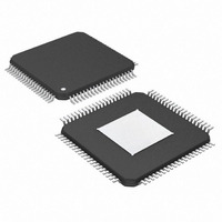
IC ADC 6BIT 800MSPS DL 80TQFP
Manufacturer
Maxim Integrated Products
Datasheet
1.MAX105ECS.pdf
(21 pages)
Specifications of MAX105ECS+
Number Of Bits
6
Sampling Rate (per Second)
800M
Data Interface
Parallel
Number Of Converters
2
Power Dissipation (max)
2.6W
Voltage Supply Source
Analog and Digital
Operating Temperature
-40°C ~ 85°C
Mounting Type
Surface Mount
Package / Case
80-TQFP Exposed Pad, 80-eTQFP, 80-HTQFP, 80-VQFP
Number Of Adc Inputs
2
Conversion Rate
800 MSPs
Resolution
6 bit
Snr
37 dB
Voltage Reference
2.5 V
Supply Voltage (max)
3.6 V
Supply Voltage (min)
3 V
Maximum Power Dissipation
3.5 W
Maximum Operating Temperature
+ 85 C
Mounting Style
SMD/SMT
Input Voltage
3.3 V
Minimum Operating Temperature
- 40 C
Lead Free Status / RoHS Status
Lead free / RoHS Compliant


ELECTRICAL CHARACTERISTICS (continued)
(AV
= 0, f
otherwise noted. Typical values are at T
CLOCK INPUTS (CLK+, CLK-)
Clock Input Resistance
Clock Input Resistance
Temperature Coefficient
Minimum Clock Input
Amplitude
LVDS OUTPUTS (P0I± TO P5I±, P0Q± TO P5Q±, A0I± TO A5I±, A0Q± TO A5Q±, DREADY+, DREADY-, DOR+, DOR-)
Differential Output Voltage
C hang e i n M ag ni tud e of V
Betw een “0” and “1” S tates
Steady-State Common Mode
Output Voltage
Change in Magnitude of V
Between “0” and “1” States
Differential Output Resistance
Output Current
DYNAMIC SPECIFICATION
Effective Number of Bits
(Note 8)
Signal-to-Noise Ratio
(Notes 10, 11)
Total Harmonic Distortion
(Note 11)
Spurious-Free Dynamic Range
CC
CLK
= AV
PARAMETER
= 802.816MHz, C
CC
I = AV
_______________________________________________________________________________________
CC
Dual, 6-Bit, 800Msps ADC with On-Chip,
Q = AV
OD
OC
L
= 1µF to AGND at REF, R
CC
R = +5V, OV
SYMBOL
TCR
∆V
V
∆V
V
ENOB
SFDR
R
OC(SS)
SNR
THD
A
CLK
OD
OD
OC
CLK
= +25°C)
CC
CLK+ and CLK- to AGND
Short output together
Short to OGNDI = OGNDQ
f
-0.5dB FS (Note 9)
f
-0.5dB FS
f
-0.5dB FS (Note 9)
f
-0.5dB FS
f
-0.5dB FS (Note 9)
f
-0.5dB FS
f
-0.5dB FS (Note 9)
f
-0.5dB FS
I = OV
IN
IN
IN
IN
IN
IN
IN
IN
= 200.018MHz at
= 400.134MHz at
= 200.018MHz at
= 400.134MHz at
= 200.018MHz at
= 400.134MHz at
= 200.018MHz at
= 400.134MHz at
CC
L
= 100Ω ±1% applied to digital LVDS outputs, T
Q = +3.3V, AGND = AGNDI = AGNDQ = AGNDR = 0, OGNDI = OGNDQ
Wideband Input Amplifier
CONDITIONS
Differential
Single-ended
Differential
Differential
Single-ended
Differential
Differential
Single-ended
Differential
Differential
Single-ended
Differential
1.125
MIN
500
247
5.4
80
35
41
-44.5
-44.5
TYP
5.75
5.65
36.7
36.5
41.5
150
A
2.5
5.8
-41
25
37
45
45
5
= T
MIN
1.375
MAX
400
±25
±25
160
-41
to T
MAX
ppm/°C
UNITS
mV
, unless
dBc
Bits
mV
mV
mV
mA
dB
dB
kΩ
Ω
V
p-p
3
Related parts for MAX105ECS+
Image
Part Number
Description
Manufacturer
Datasheet
Request
R

Part Number:
Description:
MAX7528KCWPMaxim Integrated Products [CMOS Dual 8-Bit Buffered Multiplying DACs]
Manufacturer:
Maxim Integrated Products
Datasheet:
Part Number:
Description:
Single +5V, fully integrated, 1.25Gbps laser diode driver.
Manufacturer:
Maxim Integrated Products
Datasheet:
Part Number:
Description:
Single +5V, fully integrated, 155Mbps laser diode driver.
Manufacturer:
Maxim Integrated Products
Datasheet:
Part Number:
Description:
VRD11/VRD10, K8 Rev F 2/3/4-Phase PWM Controllers with Integrated Dual MOSFET Drivers
Manufacturer:
Maxim Integrated Products
Datasheet:
Part Number:
Description:
Highly Integrated Level 2 SMBus Battery Chargers
Manufacturer:
Maxim Integrated Products
Datasheet:
Part Number:
Description:
Current Monitor and Accumulator with Integrated Sense Resistor; ; Temperature Range: -40°C to +85°C
Manufacturer:
Maxim Integrated Products
Part Number:
Description:
TSSOP 14/A�/RS-485 Transceivers with Integrated 100O/120O Termination Resis
Manufacturer:
Maxim Integrated Products
Part Number:
Description:
TSSOP 14/A�/RS-485 Transceivers with Integrated 100O/120O Termination Resis
Manufacturer:
Maxim Integrated Products
Part Number:
Description:
QFN 16/A�/AC-DC and DC-DC Peak-Current-Mode Converters with Integrated Step
Manufacturer:
Maxim Integrated Products
Part Number:
Description:
TDFN/A/65V, 1A, 600KHZ, SYNCHRONOUS STEP-DOWN REGULATOR WITH INTEGRATED SWI
Manufacturer:
Maxim Integrated Products
Part Number:
Description:
Integrated Temperature Controller f
Manufacturer:
Maxim Integrated Products
Part Number:
Description:
SOT23-6/I�/45MHz to 650MHz, Integrated IF VCOs with Differential Output
Manufacturer:
Maxim Integrated Products
Part Number:
Description:
SOT23-6/I�/45MHz to 650MHz, Integrated IF VCOs with Differential Output
Manufacturer:
Maxim Integrated Products
Part Number:
Description:
EVALUATION KIT/2.4GHZ TO 2.5GHZ 802.11G/B RF TRANSCEIVER WITH INTEGRATED PA
Manufacturer:
Maxim Integrated Products
Part Number:
Description:
QFN/E/DUAL PCIE/SATA HIGH SPEED SWITCH WITH INTEGRATED BIAS RESISTOR
Manufacturer:
Maxim Integrated Products
Datasheet: