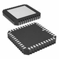
AD872AJE Analog Devices Inc, AD872AJE Datasheet - Page 11

AD872AJE
Manufacturer Part Number
AD872AJE
Description
IC ADC 12BIT 10MSPS 44-CLCC
Manufacturer
Analog Devices Inc
Datasheet
1.AD872AJD.pdf
(20 pages)
Specifications of AD872AJE
Rohs Status
RoHS non-compliant
Number Of Bits
12
Sampling Rate (per Second)
10M
Data Interface
Parallel
Number Of Converters
7
Power Dissipation (max)
1.3W
Voltage Supply Source
Analog and Digital, Dual ±
Operating Temperature
0°C ~ 70°C
Mounting Type
Surface Mount
Package / Case
44-CLCC
Available stocks
Company
Part Number
Manufacturer
Quantity
Price
REV. A
The wide input bandwidth and superior dynamic performance
of the input THA make the AD872A suitable for undersam-
pling applications where the input frequency exceeds half the
sample frequency. The input THA is designed to recover rap-
idly from input overdrive conditions, returning from a 50%
overdrive in less than 40 ns.
Because of the THA’s exceptionally wide input bandwidth,
some users may find the AD872A is sensitive to noise at fre-
quencies from 10 MHz to 50 MHz that other converters are
careful use of the differential inputs (see previous paragraphs).
Additionally, Figure 18 shows how a small capacitor (10 pF-
20 pF for 50
and V
where limiting the input bandwidth is acceptable.
The AD872A will contribute its own wideband thermal noise.
As a result of the integrated wideband noise (0.26 LSB rms,
referred-to-input), applying a dc analog input may produce
more than one code at the output. A histogram of the ADC
output codes, for a dc input voltage, will be between one and
three codes wide, depending on how well the input is centered
on a given code and how many samples are taken. Figure 8
shows a typical AD872A code histogram, and Figure 9 illus-
trates the AD872A’s transition noise.
REFERENCE INPUT
The nominal reference input should be 2.5 V, taken with re-
spect to REFERENCE GROUND (REF GND). Figure 19 il-
lustrates the equivalent model for the reference input: there is
no clock or signal-dependent activity associated with the refer-
ence input circuitry, therefore, no “kickback” into the reference.
However, in order to realize the lowest noise performance of the
AD872A, care should be taken to minimize noise at the refer-
ence input.
incapable of responding to. This sensitivity can be mitigated by
Figure 18. Optional High Frequency Noise Reduction
INB
Figure 19. Equivalent Reference Input Circuit
to help reduce high frequency noise in applications
1V
10 OR 20pF
terminated inputs) may be placed between V
REF GND
REF IN
1
2
1
2
5k
( 20%)
V
V
INA
INB
AD872A
AD872A
AV
SS
INA
–11–
The AD872A’s reference input impedance is equal to 5 k
( 20%), and its effective noise bandwidth is 10 MHz, with a
referred-to-input noise gain of 0.8. For example, the internal
reference, with an rms noise of 28 V (using an external 1 F
capacitor), contributes 24 V (0.05 LSB) of noise to the transfer
function of the AD872A.
The full-scale peak-to-peak input voltage is a function of the
reference voltage, according to the equation:
Note that the AD872A’s performance was optimized for a 2.5 V
reference input: performance may degrade somewhat for other
reference voltages. Figure 20 illustrates the S/(N+D) perfor-
mance vs. reference voltage for a 1 MHz, –0.5 dB input signal.
Note also that if the reference is changed during a conversion,
all three conversions in the pipeline will be invalidated.
Table II summarizes various 2.5 V references suitable for use
with the AD872A, including the onboard bandgap reference
(see REFERENCE OUTPUT section).
REF43B
AD680JN
Internal
If an external reference is connected to REF IN, REF OUT
must be connected to +5 V. This should lower the current in
REF GND to less than 350 A and eliminate the need for a
1 F capacitor, although decoupling the reference for noise
reduction purposes is recommended.
Alternatively, Figure 21 shows how the AD872A may be driven
from other references by use of an external resistor. The exter-
nal resistor forms a resistor divider with the on-chip 5 k resis-
tor to realize 2.5 V at the reference input pin (REF IN). A trim
potentiometer is needed to accommodate the tolerance of the
AD872A’s 5 k resistor.
(V
Figure 20. S/(N+D) vs. Reference Input Voltage,
f
IN
INA
= 1 MHz, FS = 10 MHz
75
70
65
60
55
50
1.5
V
Table II. Suitable 2.5 V References
INB
1.7
) Full Scale
Drift (ppm/ C)
6 (max)
10 (max)
30 (typ)
1.9
REFERENCE INPUT VOLTAGE – V
2.1
2.3
0.8 (V
2.5
2.7
REF
2.9
Initial Accuracy %
0.2
0.4
0.4
– REF GND )
3.1
AD872A
3.3
3.5


