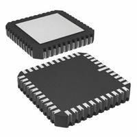
AD872AJE Analog Devices Inc, AD872AJE Datasheet - Page 12

AD872AJE
Manufacturer Part Number
AD872AJE
Description
IC ADC 12BIT 10MSPS 44-CLCC
Manufacturer
Analog Devices Inc
Datasheet
1.AD872AJD.pdf
(20 pages)
Specifications of AD872AJE
Rohs Status
RoHS non-compliant
Number Of Bits
12
Sampling Rate (per Second)
10M
Data Interface
Parallel
Number Of Converters
7
Power Dissipation (max)
1.3W
Voltage Supply Source
Analog and Digital, Dual ±
Operating Temperature
0°C ~ 70°C
Mounting Type
Surface Mount
Package / Case
44-CLCC
Available stocks
Company
Part Number
Manufacturer
Quantity
Price
AD872A
REFERENCE GROUND
The REF GND pin provides the reference point for both the
reference input, and the reference output. When the internal
reference is operating, it will draw approximately 500 A of cur-
rent through the reference ground, so a low impedance path to
the external common is desirable. The AD872A can tolerate a
fairly large difference between REF GND and AGND, up to
+1 V, without any performance degradation.
REFERENCE OUTPUT
The AD872A features an onboard, curvature compensated
bandgap reference that has been laser trimmed for both absolute
value and temperature drift. The output stage of the reference
was designed to allow the use of an external capacitor to limit
the wideband noise. As Figure 22 illustrates, a 1 F capacitor on
the reference output is required for stability of the reference output
buffer. Note: If used, an external reference may become unstable
with this capacitor in place.
With this capacitor in place, the noise on the reference output is
approximately 28 V rms at room temperature. Figure 23 shows
the typical temperature drift performance of the reference, while
Figure 24 illustrates the variation in reference voltage with load
currents.
The output stage is designed to provide at least 2 mA of out-
put current, allowing a single reference to drive up to four
AD872As, or other external loads. The power supply rejection
of the reference is better than –54 dB at dc.
Figure 22. Typical Reference Decoupling Connection
Figure 21. Optional +5 V Reference Input Circuit
+5V REF
0.1 F
1.0 F
R
2k
T
+
3.9k
R
2.5V
REF IN
REF GND
REF OUT
REF IN
REF GND
AD872A
5k
AD872A
–12–
DIGITAL OUTPUTS
In 28-lead packages, the AD872A output data is presented in
twos complement format. Table III indicates offset binary and
twos complement output for various analog inputs.
Analog Input
V
0.999268 V
0 V
–1 V
–1.000244 V
Users requiring offset binary encoding may simply invert the
MSB pin. In the 44-terminal surface mount packages, both
MSB and MSB bits are provided.
The AD872A features a digital out-of-range (OTR) bit that goes
high when the input exceeds positive full scale or falls below
negative full scale. As Table III indicates, the output bits will be
set appropriately according to whether it is an out-of-range high
0.999756 V
INA
Figure 23. Reference Output Voltage vs. Temperature
Figure 24. Reference Output Voltage vs. Output Load
–V
INB
2.50
2.48
2.46
2.44
2.42
2.40
2.55
2.54
2.53
2.52
2.51
2.50
2.49
2.48
2.47
2.46
2.45
–55
1k
Table III. Output Data Format
–35
Offset Binary
1111 1111 1111
1111 1111 1111
1000 0000 0000
0000 0000 0000
0000 0000 0000
–15
REFERENCE OUTPUT LOAD –
10k
5
TEMPERATURE – C
25
Digital Output
Twos Complement OTR
0111 1111 1111
0111 1111 1111
0000 0000 0000
1000 0000 0000
1000 0000 0000
45
100k
65
85
105
1M
REV. A
125
1
0
0
0
1


