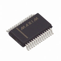
MAX1414CAI+ Maxim Integrated Products, MAX1414CAI+ Datasheet - Page 16

MAX1414CAI+
Manufacturer Part Number
MAX1414CAI+
Description
IC DAS 16BIT LP 28-SSOP
Manufacturer
Maxim Integrated Products
Type
Data Acquisition System (DAS)r
Datasheet
1.MAX1409CAP.pdf
(48 pages)
Specifications of MAX1414CAI+
Resolution (bits)
16 b
Sampling Rate (per Second)
60
Data Interface
Serial
Voltage Supply Source
Analog and Digital
Voltage - Supply
2.7 V ~ 3.6 V
Operating Temperature
0°C ~ 70°C
Mounting Type
Surface Mount
Package / Case
28-SSOP
Number Of Converters
1
Resolution
16 bit
Interface Type
Serial (4-Wire, SPI, QSPI, Microwire)
Supply Voltage (max)
3.6 V
Supply Voltage (min)
2.7 V
Maximum Power Dissipation
762 mW
Maximum Operating Temperature
+ 70 C
Mounting Style
SMD/SMT
Minimum Operating Temperature
0 C
Lead Free Status / RoHS Status
Lead free / RoHS Compliant
With the use of two external resistors, the DAC output
can go from 0.05V to AV
DACs both utilize a precise low-drift 1.25V internal
bandgap reference for conversions and setting of the
full-scale range. For applications that require increased
accuracy, power-down the internal reference and con-
nect an external reference at REF. The RTC is leap year
compensated until 9999 and provides an alarm function
that can be used to wake-up the system or cause an
interrupt at a predefined time. The power-supply volt-
age monitors detect when AV
threshold voltage at either +1.8V or +2.7V causing the
reset to be asserted. The 4-wire serial interface is used
to communicate directly between SPI, QSPI, and
MICROWIRE devices for system configuration and
readback functions.
Internal protection diodes clamp the analog input to
AV
swing from AGND - 0.3V to AV
age. However, for accurate conversions near full scale,
the inputs must not exceed AV
or be lower than AGND by 50mV.
Low-Power, 16-Bit Multichannel DAS with
Internal Reference,10-Bit DACs, and RTC
16
Figure 1. MAX1407/MAX1414 Functional Diagram
DD
______________________________________________________________________________________
and AGND, which allow the channel input pins to
DOUT
SCLK
DIN
IN3
IN2
IN1
IN0
*MAX1414 HAS A +50mV SIGNAL-DETECT COMPARATOR THRESHOLD.
CS
Analog Input Protection
DD
AGND
OUT2
OUT1
AV
REF
FB2
FB1
REF
IN3
IN2
IN1
IN0
DD
- 0.2V. The ADCs and
DD
DD
DD
INTERFACE
SERIAL
+ 0.3V without dam-
INPUT
INPUT
by more than 50mV
AV
MUX
AGND
MUX
8:1
8:1
DD
falls below a trip
CPLL
2.4576MHz
PLL
SUPERVISORS
GENERATOR
1.8V/2.7V
FOUT
RESET
RESET
BUF
BUF
µP
CLKIN CLKOUT
OSCILLATOR
32.768kHz
REFERENCE
BANDGAP
COMPARATOR
1.25V
BUF
PGA
REF
The MAX1407/MAX1408/MAX1414 include a dual 8 to 1
multiplexer for the positive and negative inputs of the
ADC. The MAX1409 has a dual 4 to 1 multiplexer at the
inputs of the ADC. Figures 1, 2, and 3 illustrate which
signals are present at the inputs of each multiplexer for
the MAX1407/MAX1408/MAX1409/MAX1414. The
MUXP and MUXN bits of the MUX register choose
which inputs will be seen at the input to the ADC
(Tables 4 and 5) and the signal-detect comparator. See
the MUX Register description under the On-Chip
Registers section for multiplexer functionality.
The MAX1407/MAX1408/MAX1409/MAX1414 provide
input buffers to isolate the analog inputs from the capaci-
tive load presented by the ADC modulator (Figure 5 and
6). The buffers are chopper stabilized to reduce the effect
of their DC offsets and low-frequency noise. Since the
buffers can represent more than 25% of the total analog
power dissipation (typically 220µA), they may be shut
down in applications where minimum power dissipation is
required and the capacitive input load is not a concern
(see ADC and Power1 Registers). Disable the buffers in
applications where the inputs must operate close to
AGND or above +1.4V. The buffers are individually
enabled or disabled.
MAX1407/MAX1414
RTC AND
ALARM
16-BIT ADC
10-BIT DAC
10-BIT DAC
GENERATOR
INTERRUPT
WAKE-UP
DIGITAL
OUTPUT
DGND
LOGIC
DV
DD
WU2
WU1
SHDN
INT
DRDY
D0
OUT1
FB1
OUT2
FB2
Input Buffers
Analog Mux


