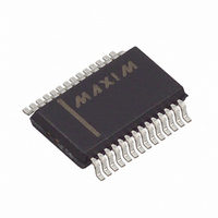
MAX1414CAI+ Maxim Integrated Products, MAX1414CAI+ Datasheet - Page 26

MAX1414CAI+
Manufacturer Part Number
MAX1414CAI+
Description
IC DAS 16BIT LP 28-SSOP
Manufacturer
Maxim Integrated Products
Type
Data Acquisition System (DAS)r
Datasheet
1.MAX1409CAP.pdf
(48 pages)
Specifications of MAX1414CAI+
Resolution (bits)
16 b
Sampling Rate (per Second)
60
Data Interface
Serial
Voltage Supply Source
Analog and Digital
Voltage - Supply
2.7 V ~ 3.6 V
Operating Temperature
0°C ~ 70°C
Mounting Type
Surface Mount
Package / Case
28-SSOP
Number Of Converters
1
Resolution
16 bit
Interface Type
Serial (4-Wire, SPI, QSPI, Microwire)
Supply Voltage (max)
3.6 V
Supply Voltage (min)
2.7 V
Maximum Power Dissipation
762 mW
Maximum Operating Temperature
+ 70 C
Mounting Style
SMD/SMT
Minimum Operating Temperature
0 C
Lead Free Status / RoHS Status
Lead free / RoHS Compliant
MODE: Conversion Mode bit. A logic zero selects a
normal ADC conversion, while a logic 1 selects an offset
calibration conversion. After completing a calibration
conversion, MODE automatically resets to zero.
RATE: Conversion Rate bit. A logic zero selects a 30Hz
conversion rate while a logic 1 selects a 60Hz conver-
sion rate.
GAIN1, GAIN0: Gain bits. The Gain bits select the PGA
gain. For an ADC gain of +1/3, +1, and 2V/V, [GAIN1
GAIN0] are 00, 01, and 10, respectively.
BUFP: Positive Buffer bit. When this bit is 0, the positive
input buffer is bypassed and powered down. When this
bit is 1 and the BUFE bit in the Power1 register is 1, the
positive input buffer drives the ADC input sampling
capacitors.
BUFN: Negative Buffer bit. When this bit is 0, the nega-
tive input buffer is bypassed and powered-down. When
this bit is 1 and the BUFE bit in the Power1 register is 1,
the negative input buffer drives the ADC input sampling
capacitors.
MUXP2, MUXP1, MUXP0: Positive Multiplexer bits.
MUXP[2:0] direct one-of-eight positive inputs to the
positive input of the ADC. Table 4 relates the MUXP bits
to the positive multiplexer inputs.
MUXN2, MUXN1, MUXN0: Negative Multiplexer bits.
MUXN[2:0] direct one-of-eight (one-of-four for the
MAX1409) negative inputs to the negative input of the
ADC. Table 5 relates the MUXN bits to the negative
multiplexer inputs.
DBIT: Digital Output bit. This bit controls the output
state of D0. When the output buffer is enabled, D0 is
low if Dbit is equal to 0, and high if Dbit is equal to 1.
D0 is enabled by the D0E bit of the Power2 register.
Low-Power, 16-Bit Multichannel DAS with
Internal Reference,10-Bit DACs, and RTC
26
NAME
DEFAULTS
NAME
DEFAULTS
______________________________________________________________________________________
FIRST BIT (MSB)
MUXP2
FIRST BIT (MSB)
MODE
0
0
MUXP1
RATE
0
0
MUXP0
GAIN1
0
0
MUXN2
GAIN0
0
0
STA2: Start bit. Setting STA2 to a logic 1 updates the
mux selection, resets the registers inside the ADC filter,
updates the ADC configuration according to the ADC
register, and initiates an analog-to-digital conversion.
The initial conversion requires three cycles for valid out-
put data, and each subsequent conversion cycle will
output valid data. STA2 automatically resets to 0 after
the initial conversion completes. The ADC will continue
to do conversions until it is powered down. Writing to
the MUX register with the STA2 bit set to 0, updates the
MUX register and selection, but leaves the ADC config-
uration unchanged. The MUX input can be switched
with the ADC continuously converting without the digital
filter resetting.
BIP: Unipolar/Bipolar bit. A logic zero selects unipolar
mode while a logic 1 selects bipolar mode.
STA1: Start bit. Setting STA1 to a logic 1 resets the reg-
isters inside the ADC filter, updates the ADC configura-
tion according to the ADC register, and initiates an
analog-to-digital conversion or offset calibration. The
initial conversion requires three cycles for valid output
data, and each subsequent conversion cycle will output
valid data. After completing the intial conversion, STA1
automatically resets to 0; however, the ADC will contin-
ue to do conversions until it is powered down.
Writing to the ADC register with STA1 set to 0 updates
the ADC register without changing the ADC configura-
tion and allows the ADC to continue conversions unin-
terrupted. This allows the ADC and MUX configuration
to be updated simultaneously. See STA2 bit of the MUX
register.
MUXN1
BUFP
0
0
MUXN0
BUFN
0
0
MUX REGISTER (00001)
ADC REGISTER (00000)
On-Chip Registers
DBIT
BIP
0
0
(LSB)
(LSB)
STA2
STA1
0
0


