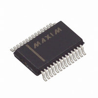
MAX1414CAI+ Maxim Integrated Products, MAX1414CAI+ Datasheet - Page 46

MAX1414CAI+
Manufacturer Part Number
MAX1414CAI+
Description
IC DAS 16BIT LP 28-SSOP
Manufacturer
Maxim Integrated Products
Type
Data Acquisition System (DAS)r
Datasheet
1.MAX1409CAP.pdf
(48 pages)
Specifications of MAX1414CAI+
Resolution (bits)
16 b
Sampling Rate (per Second)
60
Data Interface
Serial
Voltage Supply Source
Analog and Digital
Voltage - Supply
2.7 V ~ 3.6 V
Operating Temperature
0°C ~ 70°C
Mounting Type
Surface Mount
Package / Case
28-SSOP
Number Of Converters
1
Resolution
16 bit
Interface Type
Serial (4-Wire, SPI, QSPI, Microwire)
Supply Voltage (max)
3.6 V
Supply Voltage (min)
2.7 V
Maximum Power Dissipation
762 mW
Maximum Operating Temperature
+ 70 C
Mounting Style
SMD/SMT
Minimum Operating Temperature
0 C
Lead Free Status / RoHS Status
Lead free / RoHS Compliant
the placement of the crystal on the PC board layout to
insure that extra clock “ticks” do not couple onto the
crystal pins.
1) It is important to place the crystal as close as possi-
2) Keep the crystal bond pads and trace width to the
3) If possible, place a guard ring (connect to ground)
4) Insure that no signals on other PC board layers run
Low-Power, 16-Bit Multichannel DAS with
Internal Reference,10-Bit DACs, and RTC
46
ble to the CLKIN and CLKOUT pins. Keeping the
trace lengths between the crystal and pins as small
as possible reduces the probability of noise cou-
pling by reducing the length of the “antennae”.
Keeping the trace lengths small also decreases the
amount of stray capacitance.
CLKIN and CLKOUT pins as small as possible. The
larger these bond pads and traces are, the more
likely it is that noise can couple from adjacent signals.
around the crystal. This helps to isolate the crystal
from noise coupled from adjacent signals.
directly below the crystal or below the traces to the
CLKIN and CLKOUT pins. The more the crystal is
isolated from other signals on the board, the less
likely it is that noise will be coupled into the crystal.
There should be a minimum of 0.200 inches
between any digital signal and any trace connected
______________________________________________________________________________________
TOP VIEW
RESET
AGND
AV
CPLL
WU1
WU2
REF
IN7
IN6
IN4
IN0
IN1
IN2
DO
DD
10
11
12
13
14
1
2
3
4
5
6
7
8
9
MAX1408
28
27
26
25
24
23
22
21
20
19
18
17
16
15
IN5
IN3
DV
DGND
SCLK
DIN
DOUT
INT
CLKIN
CLKOUT
FOUT
DRDY
SHDN
CS
DD
RESET
AGND
OUT1
5) It may also be helpful to place a local ground plane
Integral nonlinearity (INL) is the deviation of the values
on an actual transfer function (with offset and gain error
removed) from a straight line. This straight line can be
either a best straight-line fit or a line drawn between the
endpoints of the transfer function, once offset and gain
errors have been nullified. The static linearity parame-
ters for the MAX1407/MAX1408/MAX1409/MAX1414 are
measured using the endpoint method.
Differential nonlinearity (DNL) is the difference between
an actual step width and the ideal value of 1LSB. A
DNL error specification of less than 1LSB guarantees
no missing codes and a monotonic transfer function.
AV
CPLL
WU1
WU2
FB1
REF
IN0
DD
to CLKIN or CLKOUT.
on the PC board layer immediately below the crystal
guard ring. This helps to isolate the crystal from
noise coupling from signals on other PC board lay-
ers. Note: The ground plane needs to be in the
vicinity of the crystal only and not on the entire
board.
10
1
2
3
4
5
6
7
8
9
Pin Configurations (continued)
MAX1409
20
19
18
17
16
15
14
13
12
11
DV
DGND
CS
SCLK
DIN
DOUT
CLKIN
CLKOUT
FOUT
INT
DD
Differential Nonlinearity
Integral Nonlinearity
Definitions


