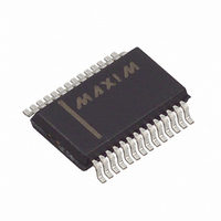
MAX1414CAI+ Maxim Integrated Products, MAX1414CAI+ Datasheet - Page 21

MAX1414CAI+
Manufacturer Part Number
MAX1414CAI+
Description
IC DAS 16BIT LP 28-SSOP
Manufacturer
Maxim Integrated Products
Type
Data Acquisition System (DAS)r
Datasheet
1.MAX1409CAP.pdf
(48 pages)
Specifications of MAX1414CAI+
Resolution (bits)
16 b
Sampling Rate (per Second)
60
Data Interface
Serial
Voltage Supply Source
Analog and Digital
Voltage - Supply
2.7 V ~ 3.6 V
Operating Temperature
0°C ~ 70°C
Mounting Type
Surface Mount
Package / Case
28-SSOP
Number Of Converters
1
Resolution
16 bit
Interface Type
Serial (4-Wire, SPI, QSPI, Microwire)
Supply Voltage (max)
3.6 V
Supply Voltage (min)
2.7 V
Maximum Power Dissipation
762 mW
Maximum Operating Temperature
+ 70 C
Mounting Style
SMD/SMT
Minimum Operating Temperature
0 C
Lead Free Status / RoHS Status
Lead free / RoHS Compliant
The MAX1407/MAX1408/MAX1409/MAX1414 have an
internal low-drift +1.25V reference used for both ADC
and DAC conversion. The buffered reference output
can be used as a reference source for other devices in
the system. The internal reference requires a 4.7µF low-
ESR ceramic capacitor or tantalum capacitor connect-
ed between REF and AGND. For applications that
require increased accuracy, power-down the internal
reference by writing a 0 to the REFE bit of the Power1
register and connect an external reference source to
REF. The valid external reference voltage range is
1.25V ±100mV.
The on-chip oscillator requires an external crystal (or
resonator) connected between CLKIN and CLKOUT
with an operating frequency of 32.768kHz. This oscilla-
tor is used for the RTC, alarm, signal-detect compara-
tor, and PLL. The oscillator is operational down to 1.8V.
In any crystal-based oscillator circuit, the oscillator fre-
quency is based on the characteristics of the crystal. It
is important to select a crystal that meets the design
requirements, especially the capacitive load (C
must be placed across the crystal pins in order for the
crystal to oscillate at its specified frequency. C
capacitance that the crystal needs to “see” from the
oscillator circuit; it is not the capacitance of the crystal
itself. The MAX1407/MAX1408/MAX1409/MAX1414
have 6pF of capacitance across the CLKIN and CLK-
OUT pins. Choose a crystal with a 32.768kHz oscillation
frequency and a 6pF capacitive load such as the C-
002RX32-E from Epson Crystal. Using a crystal with a
C
lator circuit will cause the oscillator to run faster than
the specified nominal frequency of the crystal.
Conversely, using a crystal with a C
than the load capacitance of the oscillator circuit will
cause the oscillator to run slower than the specified
nominal frequency of the crystal.
An on-board phase-locked loop generates a
2.4576MHz clock at FOUT from the 32.768kHz crystal
oscillator. FOUT can be used to clock a µP or other dig-
ital circuitry. Connect an 18nF ceramic capacitor from
CPLL to AV
FOUT. To power down the PLL, clear PLLE in the
Power2 register (see Power2 Register) or write to the
Sleep register. FOUT will be active for 1.95ms (t
after receiving either power-down command and then
go low. This provides extra clock signals to the µP to
complete a shutdown sequence. The PLL is active in all
L
that is larger than the load capacitance of the oscil-
Phase-Locked Loop (PLL) and FOUT
DD
to create the 2.4576MHz clock signal at
Low-Power, 16-Bit Multichannel DAS with
Internal Reference,10-Bit DACs, and RTC
______________________________________________________________________________________
Internal/External Reference
Crystal Oscillator
L
that is smaller
L
L
DFOF
is the
) that
)
modes except the sleep mode (see Power Modes). To
reactivate the PLL, the following conditions must be
met: AV
threshold, RESET is deasserted, and the PLLE bit is
equal to “1”. FOUT is enabled 31.25ms (t
the PLL is activated. At initial power-up, the PLL is
enabled. If RESET is asserted while the PLL is running,
the PLL does not shut down.
The integrated RTC provides the current second,
minute, hour, date, month, day, year, century, and mil-
lenium information. An internally generated reference
clock of 1.024kHz (derived from the 32.768kHz crystal)
drives the RTC. The RTC operates in either 24-hour or
12-hour format with an AM/PM indicator (see RTC_Hour
Register). An internal calendar compensates for months
with less than 31 days and includes leap year correc-
tion through the year 9999. The RTC operates from a
supply voltage of +1.8V to +3.6V and consumes less
than 1µA current.
The MAX1407/MAX1408/MAX1409/MAX1414 offer a time
of day alarm which generates an interrupt when the RTC
reaches a preset combination of seconds, minutes,
hours, and day (see Alarm Registers). In addition to set-
ting a “single-shot” alarm, the Time of Day Alarm can
also be programmed to generate an alarm every sec-
ond, minute, hour, day, or week. “Don’t care” states can
be inserted into one or more fields if it is desired for them
to be ignored for the alarm condition. The Time of Day
Alarm wakes up the device into Standby mode if it is in
Sleep mode. The Time of Day Alarm operates from a
supply voltage of +1.8V to +3.6V.
INT indicates one of three conditions. After receiving a
valid interrupt (INT goes low), read the Status register
and the Al_Status register (if the alarm is enabled) to
identify the source of the interrupt. The three sources of
interrupts are from the CLK, SDC, and ALIRQ bits.
On power-up, INT is high. 7.82ms (t
output appears on FOUT, INT goes low (see Figure 15).
The CLK bit of the Status register is set to “1” after
FOUT is enabled. Reading the Status register clears the
CLK bit. INT remains low until the device detects a start
bit through the serial interface from the µP. The purpose
of this interrupt is to inform the µP that the FOUT clock
signal is present.
DD
is greater than the low V
Real-Time Clock (RTC)
Time of Day Alarm
DD
DFI
Interrupt ( I I N N T T )
voltage monitor
) after the PLL
DFON
PLL Ready
) after
21


