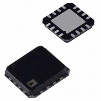
AD7879ACPZ-RL Analog Devices Inc, AD7879ACPZ-RL Datasheet - Page 28

AD7879ACPZ-RL
Manufacturer Part Number
AD7879ACPZ-RL
Description
IC ADC 12BIT CTLR TOUCH 16LFCSP
Manufacturer
Analog Devices Inc
Type
Touch Screen Controller: 4-Wire Resistiver
Datasheet
1.AD7879-1ACPZ-RL.pdf
(36 pages)
Specifications of AD7879ACPZ-RL
Resolution (bits)
12 b
Data Interface
I²C
Package / Case
16-LFCSP
Mounting Type
Surface Mount
Voltage - Supply
1.6 V ~ 3.6 V
Operating Temperature
-40°C ~ 85°C
Voltage Supply Source
Single Supply
Sampling Rate (per Second)
105k
Sampling Rate
105kSPS
Supply Voltage Range - Analog
1.6V To 3.6V
Supply Current
480µA
Digital Ic Case Style
CSP
No. Of Pins
16
Lead Free Status / RoHS Status
Lead free / RoHS Compliant
Available stocks
Company
Part Number
Manufacturer
Quantity
Price
Company:
Part Number:
AD7879ACPZ-RL
Manufacturer:
Maxim
Quantity:
50
AD7879
INTERRUPTS
The AD7879 has a dual function interrupt output, INT , as well
as a pen down interrupt, PENIRQ . The INT output can be con-
figured as a data available interrupt, as an out of limit interrupt, or
as a GPIO interrupt.
INT —Data Available
The behavior of the interrupt output is controlled by Bit 13 in
Control Register 3. In default mode, INT operates as a data
available interrupt (Bit 13 = 0). When the AD7879 has finished
a conversion or a conversion sequence, the interrupt asserts to
let the host know that new ADC data is available in the result
registers.
While the ADC is idle or is converting, INT is high. When the
ADC has finished converting and new data has been written to
the results registers, INT goes low. Reading the result registers
COMPARISON
OUT-OF-
NO
LIMIT?
LIMIT
NO
COMPARE NEW
RUN FILTER
AVERAGER
READINGS
FINISHED?
READING
WINDOW
MEDIAN
YES
SHIFT
CONVERSION
SEQUENCE
YES
START OF
Figure 33. Conversion Sequence
START FCD
WAIT FOR
SET ALERT AND
TIMER
INTERRUPT
FCD
YES
YES
START ACQUIST TIMER
CONVERT: WAIT FOR
CONV_START = 1
CONV_START = 0
EOCS
SET CHANNEL
AND WAIT FOR
DATA_READY
TO REG. MAP
ACQUISITION
TXFER DATA
MAV FILTER
AVERAGER
?
FINISHED?
ENABLED
YES
NO
REQ’D?
FCD
RUN
AVG
NO
NO
NOTE THAT CONVERSION
SEQUENCE MAY BE 1
CHANNEL ONLY (MODE 01).
YES
NO
CONVERSION
SEQUENCE
NO FCD
END OF
REQ’D
Rev. 0 | Page 28 of 36
resets INT to a high condition. INT is also reset if a new conver-
sion is started by the AD7879 because the timer expired. The
host should read the results registers only when INT is low. To
ensure correct operation of the DAV mode when using the SPI
interface it is necessary to write 0x0000 to Register 0x81 after a
set of register reads. This clears the internal data read signal.
AD7879
When the on-board timer is programmed to perform automatic
conversions, limited time is available to the host to read the
results registers before another sequence of conversions begins.
The INT signal is reset high when the timer expires, and the
host should not access the results registers while INT is high.
INT —Out of Limits
The INT pin operates as an alarm or interrupt output when
Bit 13 in Register 0x03 is set to 1. The output goes low if any
one of the interrupt sources is asserted. The results of high and
low limit comparisons on the AUX, VBAT, and TEMP channels
are interrupt sources. An out-of-limit comparison sets a status
bit in the interrupt register. There are separate status bits for
both the high and low limits on each channel to indicate which
limit was exceeded. The interrupt sources can be masked by
clearing the corresponding enable bit in this register. There is
one enable bit per channel.
PENIRQ — Pen Interrupt
The pen interrupt request output ( PENIRQ ) goes low when-
ever the screen is touched and the PENIRQ enable bit is set to
0 (Control Register 1, Bit 15). When PENIRQ enable is set to 1,
the pen interrupt request output is disabled.
The pen interrupt equivalent output circuitry is outlined in
Figure 35. This is a digital logic output with an internal 50 kΩ
pull-up resistor, which means it does not need an external pull-
up. The PENIRQ output idles high, and the PENIRQ circuitry
is always enabled in master mode (ADC mode = 11), except
during conversions.
STATUS
X–
INT
IDLE
SCREEN
TOUCH
Figure 35. PENIRQ Output Equivalent Circuit
BY HOST
SETUP
Figure 34. Operation of INT Output
CONVERTING
X+
t
Y+
Y–
CONV
ADC
ENABLE
PENIRQ
V
CC
AVAILABLE
NEW DATA
50kΩ
V
CC
HOST READS
RESULTS
PENIRQ
IDLE


