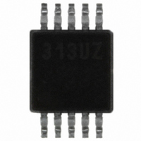
ISL22313UFU10Z Intersil, ISL22313UFU10Z Datasheet - Page 13

ISL22313UFU10Z
Manufacturer Part Number
ISL22313UFU10Z
Description
IC POT DGTL 256TP LN LP 10-MSOP
Manufacturer
Intersil
Series
XDCP™r
Datasheet
1.ISL22313UFU10Z.pdf
(15 pages)
Specifications of ISL22313UFU10Z
Taps
256
Resistance (ohms)
50K
Number Of Circuits
1
Temperature Coefficient
50 ppm/°C Typical
Memory Type
Non-Volatile
Interface
I²C, 2-Wire Serial
Voltage - Supply
2.25 V ~ 5.5 V
Operating Temperature
-40°C ~ 125°C
Mounting Type
Surface Mount
Package / Case
10-MSOP, Micro10™, 10-uMAX, 10-uSOP
Resistance In Ohms
50K
Lead Free Status / RoHS Status
Lead free / RoHS Compliant
Available stocks
Company
Part Number
Manufacturer
Quantity
Price
Company:
Part Number:
ISL22313UFU10Z
Manufacturer:
Intersil
Quantity:
1 769
Write Operation
A Write operation requires a START condition, followed by a
valid Identification Byte, a valid Address Byte, a Data Byte,
and a STOP condition. After each of the three bytes, the
ISL22313 responds with an ACK. At this time, the device
enters its standby state (see Figure 18).
The non-volatile write cycle starts after STOP condition is
determined and it requires up to 20ms delay for the next
non-volatile write. Thus, non-volatile registers must be
written individually.
SIGNAL AT SDA
FROM THE
SIGNALS
MASTER
SIGNALS FROM
SDA OUTPUT FROM
SDA OUTPUT FROM
THE SLAVE
TRANSMITTER
S
A
R
T
T
SCL FROM
RECEIVER
MASTER
1
IDENTIFICATION
0
BYTE WITH
SIGNALS FROM
SIGNAL AT SDA
SIGNALS FROM
1
R/W = 0
THE MASTER
0
THE SLAVE
13
0
A1
START
A0
0
FIGURE 17. ACKNOWLEDGE RESPONSE FROM RECEIVER
A
C
K
0 0 0
HIGH IMPEDANCE
ADDRESS
S
A
R
T
T
BYTE
0
FIGURE 18. BYTE WRITE SEQUENCE
1
IDENTIFICATION
0
1
FIGURE 19. READ SEQUENCE
1
BYTE
0
0
A1
A
C
K
ISL22313
A0
A
R
S
T
T
WRITE
0
1 0 1 0
IDENTIFICATION
A
C
K
BYTE WITH
R/W = 1
0 0 0 0
ADDRESS
Read Operation
A Read operation consist of a three byte instruction followed
by one or more Data Bytes (see Figure 19). The master
initiates the operation issuing the following sequence: a
START, the Identification byte with the R/W bit set to “0”, an
Address Byte, a second START, and a second Identification
byte with the R/W bit set to “1”. After each of the three bytes,
the ISL22313 responds with an ACK. Then the ISL22313
transmits Data Bytes as long as the master responds with an
ACK during the SCL cycle following the eighth bit of each
byte. The Data Bytes are from the registers indicated by an
internal pointer. This pointer initial value is determined by the
Address Byte in the Read operation instruction, and
0
BYTE
A1
0
A0
1
A
C
K
A
C
K
8
FIRST READ
DATA BYTE
DATA
BYTE
A
C
K
HIGH IMPEDANCE
ACK
9
A
C
K
A
C
K
S
T
O
P
LAST READ
DATA BYTE
July 17, 2007
A
C
K
FN6421.0
S
T
O
P


