X9252WV24IZ-2.7 Intersil, X9252WV24IZ-2.7 Datasheet - Page 13
X9252WV24IZ-2.7
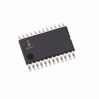
Manufacturer Part Number
X9252WV24IZ-2.7
Description
IC POT DGTL QUAD 24-TSSOP
Manufacturer
Intersil
Series
XDCP™r
Datasheet
1.X9252YV24IZ-2.7.pdf
(20 pages)
Specifications of X9252WV24IZ-2.7
Taps
256
Resistance (ohms)
10K
Number Of Circuits
4
Temperature Coefficient
300 ppm/°C Typical
Memory Type
Non-Volatile
Interface
I²C, 2-Wire Serial
Voltage - Supply
2.7 V ~ 5.5 V
Operating Temperature
-40°C ~ 85°C
Mounting Type
Surface Mount
Package / Case
24-TSSOP
Resistance In Ohms
10K
Track Taper
Linear
Resistance Tolerance
± 20%
No. Of Steps
256
Supply Voltage Range
2.7V To 5.5V
Control Interface
2 Wire, Serial
No. Of Pots
Quad
Rohs Compliant
Yes
Lead Free Status / RoHS Status
Lead free / RoHS Compliant
Available stocks
Company
Part Number
Manufacturer
Quantity
Price

Part Number:
X9252WV24IZ-2.7
Manufacturer:
INTERSIL
Quantity:
20 000


DCP Addressing for 2-Wire Interface
Once the register number has been selected by a 2-wire
instruction, then the DCP number is determined by the
Address Byte of the following instruction. Note again that this
enables a complete page write of the DRs of all four
potentiometers at once. The register addresses accessible
in the X9252 include:
All other address bits in the Address Byte must be set to “0”
during 2-wire write operations and their value should be
ignored when read.
Byte Write Operation
For any Byte Write operation, the X9252 requires the Slave
Address byte, an Address Byte, and a Data Byte (See Figure
7). After each of them, the X9252 responds with an ACK.
The master then terminates the transfer by generating a
STOP condition. At this time, if the write operation is to a
volatile register (WCR, or SR), the X9252 is ready for the
next read or write operation. If the write operation is to a
nonvolatile register (DR), and the WP pin is high, the X9252
begins the internal write cycle to the nonvolatile memory.
During the internal nonvolatile write cycle, the X9252 does
ADDRESS (HEX)
TABLE 3. 2-WIRE INTERFACE ADDRESS BYTE
0
1
2
3
4
5
6
7
Signals from the
Signals from the
Signal at SDA
13
Master
Slave
Status Register
CONTENTS
Not Used
Not Used
Not Used
DCP 0
DCP 1
DCP 2
DCP 3
S
a
t
r
t
0
1
FIGURE 7. BYTE WRITE SEQUENCE
0
Address
Slave
1
0
Write
X9252
A
C
K
Address
not respond to any requests from the master. The SDA
output is at high impedance.
The SR bits and WP pin determine the register being
accessed through the 2-wire interface (See Table 2).
As noted before, any write operation to a Data Register
(DR), also transfers the contents of all the data registers in
that row to their corresponding WCR.
For example, to write 3Ahex to the Data Register 1 of DCP2
the following sequence is required:
During the sequence of this example, WP pin must be high,
and A0, A1, and A2 pins must be low. When completed, the
DR21 register and the WCR2 will be set to 3Ah and the other
Data Register in Row 1 will transfer their other contents to
the respective WCR’s.
START
Slave Address
ACK
Address Byte
ACK
Data Byte
ACK
note: at this ACK, the WCRs are all updated with their respective DR.
STOP
START
Slave Address
ACK
Address Byte
ACK
Data Byte
ACK
STOP
Byte
A
C
K
0101 0000
0000 0111
0000 0011
0101 0000
0000 0010
0011 1010
Data
Byte
A
C
K
(Hardware Address = 000,
and a Write command)
(Indicates Status Register
address)
(Data Register 1 and
NVEnable selected)
(Hardware address = 000,
Write command)
(Access DCP2)
(Write Data Byte 3Ah)
S
o
p
t
November 14, 2005
FN8167.2
Related parts for X9252WV24IZ-2.7
Image
Part Number
Description
Manufacturer
Datasheet
Request
R

Part Number:
Description:
IC DCP QUAD 10K 256TAP 24-TSSOP
Manufacturer:
Intersil
Datasheet:

Part Number:
Description:
Intersil Corporation [CMOS Serial Controller Interface]
Manufacturer:
Intersil Corporation
Datasheet:
Part Number:
Description:
Manufacturer:
Intersil Corporation
Datasheet:
Part Number:
Description:
357-036-542-201 CARDEDGE 36POS DL .156 BLK LOPRO
Manufacturer:
Intersil Corporation
Datasheet:
Part Number:
Description:
1024-Word x 4-Bit LSI Static RAM
Manufacturer:
Intersil Corporation
Datasheet:
Part Number:
Description:
General Purpose NPN Transistor Arrays FN341.4
Manufacturer:
Intersil Corporation
Datasheet:
Part Number:
Description:
CMOS 16-Bit Microprocessor
Manufacturer:
Intersil Corporation
Datasheet:
Part Number:
Description:
Manufacturer:
Intersil Corporation
Datasheet:
Part Number:
Description:
Manufacturer:
Intersil Corporation
Datasheet:
Part Number:
Description:
Manufacturer:
Intersil Corporation
Datasheet:
Part Number:
Description:
Manufacturer:
Intersil Corporation
Datasheet:
Part Number:
Description:
CMOS 6-Bit Latch and Decoder Memory Interfaces
Manufacturer:
Intersil Corporation
Datasheet:
Part Number:
Description:
CA3046General Purpose NPN Transistor Arrays
Manufacturer:
Intersil Corporation
Datasheet:
Part Number:
Description:
Manufacturer:
Intersil Corporation
Datasheet:
Part Number:
Description:
TR909 DLC/FLC SLIC with Low Power Standby
Manufacturer:
Intersil Corporation
Datasheet: