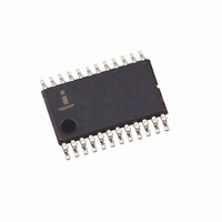
X9252WV24IZ-2.7 Intersil, X9252WV24IZ-2.7 Datasheet - Page 15

X9252WV24IZ-2.7
Manufacturer Part Number
X9252WV24IZ-2.7
Description
IC POT DGTL QUAD 24-TSSOP
Manufacturer
Intersil
Series
XDCP™r
Datasheet
1.X9252YV24IZ-2.7.pdf
(20 pages)
Specifications of X9252WV24IZ-2.7
Taps
256
Resistance (ohms)
10K
Number Of Circuits
4
Temperature Coefficient
300 ppm/°C Typical
Memory Type
Non-Volatile
Interface
I²C, 2-Wire Serial
Voltage - Supply
2.7 V ~ 5.5 V
Operating Temperature
-40°C ~ 85°C
Mounting Type
Surface Mount
Package / Case
24-TSSOP
Resistance In Ohms
10K
Track Taper
Linear
Resistance Tolerance
± 20%
No. Of Steps
256
Supply Voltage Range
2.7V To 5.5V
Control Interface
2 Wire, Serial
No. Of Pots
Quad
Rohs Compliant
Yes
Lead Free Status / RoHS Status
Lead free / RoHS Compliant
Available stocks
Company
Part Number
Manufacturer
Quantity
Price
Part Number:
X9252WV24IZ-2.7
Manufacturer:
INTERSIL
Quantity:
20 000
Move/Read Operation
The Move/Read operation simultaneously reads the
contents of a Data Register (DR) and moves the contents
into the corresponding DCP’s WCR and the WCRs of all
DCPs are updated with the content of their corresponding
DR. Move/Read operation consists of a one byte, or three
byte instruction followed by one or more Data Bytes (See
Figure 9). To read an arbitrary byte, the master initiates the
operation issuing the following sequence: a START, the
Slave Address byte with the R/W bit set to “0”, an Address
Byte, a second START, and a second Slave Address byte
with the R/W bit set to “1”. After each of the three bytes, the
X9252 responds with an ACK. Then the X9252 transmits
Signal at SDA
Signals from the
from the
Signals
Master
Slave
S
a
t
r
t
0
1
Address with
0
Setting the Current Address
R/W=0
1
Slave
15
0
A
C
K
Address
Byte
FIGURE 9. MOVE/READ SEQUENCE
A
C
K
S
a
r
t
t
Random Address Read
X9252
0
Address with
1
0
R/W=1
Slave
1
Data Bytes as long as the master responds with an ACK
during the SCL cycle following the eight bit of each byte. The
master terminates the Move/Read operation (issuing a
STOP condition) following the last bit of the last Data Byte.
The first byte being read is determined by the current DCP
address and by the Status Register bits, according to Table
2. If more than one byte is read, the DCP address is
incremented by one after each byte, in the same way as
during a Page Write operation. After reaching DCP3, the
DCP address “rolls over” to DCP0.
On power up, the Address pointer is set to the Data Register
0 of DCP0.
1
A
C
K
First Read Data
Current Address Read
Byte
One or more Data Bytes
A
C
K
A
C
K
Last Read Data
Byte
November 14, 2005
FN8167.2
S
o
p
t


