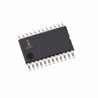
X9252WV24IZ-2.7 Intersil, X9252WV24IZ-2.7 Datasheet - Page 3

X9252WV24IZ-2.7
Manufacturer Part Number
X9252WV24IZ-2.7
Description
IC POT DGTL QUAD 24-TSSOP
Manufacturer
Intersil
Series
XDCP™r
Datasheet
1.X9252YV24IZ-2.7.pdf
(20 pages)
Specifications of X9252WV24IZ-2.7
Taps
256
Resistance (ohms)
10K
Number Of Circuits
4
Temperature Coefficient
300 ppm/°C Typical
Memory Type
Non-Volatile
Interface
I²C, 2-Wire Serial
Voltage - Supply
2.7 V ~ 5.5 V
Operating Temperature
-40°C ~ 85°C
Mounting Type
Surface Mount
Package / Case
24-TSSOP
Resistance In Ohms
10K
Track Taper
Linear
Resistance Tolerance
± 20%
No. Of Steps
256
Supply Voltage Range
2.7V To 5.5V
Control Interface
2 Wire, Serial
No. Of Pots
Quad
Rohs Compliant
Yes
Lead Free Status / RoHS Status
Lead free / RoHS Compliant
Available stocks
Company
Part Number
Manufacturer
Quantity
Price
Part Number:
X9252WV24IZ-2.7
Manufacturer:
INTERSIL
Quantity:
20 000
Pin Descriptions
Pin Descriptions
Bus Interface Pins
Serial Data Input/Output (SDA)
The SDA is a bidirectional serial data input/output pin for the
2-wire interface. It receives device address, operation code,
wiper register address and data from a 2-wire external master
device at the rising edge of the serial clock SCL, and it shifts
out data after each falling edge of the serial clock SCL.
SDA requires an external pull-up resistor, since it’s an open
drain output.
Serial Clock (SCL)
This input is the serial clock of the 2-wire and Up/Down
interface.
Device Address (A2-A0)
The Address inputs are used to set the least significant 3 bits of
the 8-bit 2-wire interface slave address. A match in the slave
address serial data stream must be made with the Address
input pins in order to initiate communication with the X9252. A
maximum of 8 devices may occupy the 2-wire serial bus.
Chip Select (CS)
When the CS pin is low, increment or decrement operations
are possible using the SCL and U/D pins. The 2-wire
SOIC/TSSOP PIN
10
12
13
14
15
16
17
18
19
20
21
22
23
24
11
5
6
7
8
9
(Continued)
SYMBOL
VCC
RW0
RW1
RW2
RH0
SDA
RH1
VSS
RH2
SCL
DS1
RL3
RL0
RL1
RL2
U/D
WP
CS
A2
A1
3
Low terminal of DCP3.
Increment/decrement for up/down interface.
System supply voltage
Low terminal of DCP0.
High terminal of DCP0.
Wiper terminal of DCP0.
Device address for 2-wire bus.
Hardware write protect
Serial data input/output for 2-wire bus.
Device address for 2-wire bus.
Low terminal of DCP1.
High terminal of DCP1.
Wiper terminal DCP1.
System ground
Chip select for Up/Down interface.
Wiper terminal of DCP2.
High terminal of DCP2.
Low terminal of DCP2.
Serial clock for 2-wire bus.
DCP select for up/down interface.
X9252
interface is disabled at this time. When CS is high, the 2-wire
interface is enabled.
Up or Down Control (U/D)
The U/D input pin is held HIGH during increment operations
and held LOW during decrement operations.
DCP Select (DS1-DS0)
The DS1-DS0 select one of the four DCPs for an Up/Down
interface operation.
Hardware Write Protect Input (WP)
When the WP pin is set low, “write” operations to non volatile
DCP Data Registers are disabled. This includes both 2-wire
interface non-volatile “Write”, and Up/Down interface “Store”
operations.
DCP Pins
R
These pins are equivalent to the terminal connections on
mechanical potentiometers. Since there are 4 DCPs, there is
one set of R
R
The wiper pins are equivalent to the wiper terminal of
mechanical potentiometers. Since there are four DCPs,
there are 4 R
H0
W0
, R
BRIEF DESCRIPTION
, R
L0
W1
, R
, R
H
H1
W
W2
and R
, R
pins.
, and R
L1
, R
L
for each DCP.
H2
W3
, R
L2
, R
H3
, and R
L3
November 14, 2005
FN8167.2


