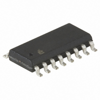
X9420YS16I Intersil, X9420YS16I Datasheet - Page 12

X9420YS16I
Manufacturer Part Number
X9420YS16I
Description
IC XDCP SGL 64-TAP 2.5K 16-SOIC
Manufacturer
Intersil
Series
XDCP™r
Datasheet
1.X9420WV14I-2.7.pdf
(19 pages)
Specifications of X9420YS16I
Taps
64
Resistance (ohms)
2.5K
Number Of Circuits
1
Temperature Coefficient
300 ppm/°C Typical
Memory Type
Non-Volatile
Interface
SPI, 3-Wire Serial
Voltage - Supply
4.5 V ~ 5.5 V
Operating Temperature
-40°C ~ 85°C
Mounting Type
Surface Mount
Package / Case
16-SOIC (0.300", 7.5mm Width)
Resistance In Ohms
2.5K
Number Of Elements
1
# Of Taps
64
Resistance (max)
2.5KOhm
Power Supply Requirement
Dual
Interface Type
Serial (SPI)
Single Supply Voltage (typ)
Not RequiredV
Dual Supply Voltage (typ)
±5V
Single Supply Voltage (min)
Not RequiredV
Single Supply Voltage (max)
Not RequiredV
Dual Supply Voltage (min)
±4.5V
Dual Supply Voltage (max)
±5.5V
Operating Temp Range
-40C to 85C
Operating Temperature Classification
Industrial
Mounting
Surface Mount
Pin Count
16
Package Type
SOIC W
Lead Free Status / RoHS Status
Contains lead / RoHS non-compliant
D.C. OPERATING CHARACTERISTICS (Over the recommended operating conditions unless otherwise specified.)
ENDURANCE AND DATA RETENTION
CAPACITANCE
POWER-UP TIMING
POWER-UP REQUIREMENTS (Power-up sequencing can affect correct recall of the wiper registers)
The preferred power-on sequence is as follows: First V
and R
specification should be met, and any glitches or slope changes in the V
If V
proper wiper register recall. Also, V
be complete until V
Notes: (5) This parameter is periodically sampled and not 100% tested.
Symbol
I
I
Symbol
Symbol
V
C
t
V
CC
CC1
CC2
I
I
t
V
PUW
t
SB
I
LO
PUR
C
R
LI
OL
OUT
IH
IL
IN
V
W
(6) t
powers down, it should be held below 0.1V for more than 1 second before powering up again in order for
CC
(5)
. Voltage should not be applied to the potentiometer pins before V+ or V- is applied. The V
(6)
(6)
(5)
can be issued. These parameters are periodically sampled and not 100% tested.
Minimum Endurance
PUR
V
V
(Non-volatile Write)
V
Input Leakage Current
Output Leakage Current
Input HIGH Voltage
Input LOW Voltage
Output LOW Voltage
Data Retention
CC
CC
CC
Parameter
and t
Supply Current (Active)
Supply Current
Current (Standby)
PUW
Power-up to Initiation of Read Operation
Power-up to Initiation of Write Operation
CC
Parameter
Input Capacitance (A0, SI, and SCK)
, V+ and V- reach their final value.
are the delays required from the time the third (last) power supply (V
12
Output Capacitance (SO)
V
CC
Parameter
Power-up Ramp
CC
Test
should not reverse polarity by more than 0.5V. Recall of wiper position will not
V
CC
Min.
-0.5
x 0.7
100,000
Min.
100
X9420
CC
Typ.
, then V+ and V-, and then the potentiometer pins, R
Limits
V
V
CC
CC
Max.
400
0.4
10
10
1
1
Max.
Max.
+ 0.5
x 0.1
0.2
1
5
8
6
CC
line should be held to <100mV if possible.
Units
Data Changes per Bit per Register
mA
CC
µA
μA
μA
μA
V
V
V
, V+ or V-) is stable until the specific instruction
Units
Max.
pF
pF
50
1
5
f
Other Inputs = V
f
Other Inputs = V
SCK = SI = V
V
V
I
SCK
SCK
OL
IN
OUT
= 3mA
= V
Units
Years
= 2MHz, SO = Open,
= 2MHz, SO = Open,
= V
Test Conditions
SS
SS
to V
Test Conditions
to V
SS
CC
V
, Addr. = V
SS
SS
V
OUT
CC
V/msec
Units
IN
CC
ms
ms
= 0V
= 0V
ramp rate
April 26, 2006
H
FN8195.1
SS
, R
L
,


