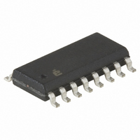
X9420YS16I Intersil, X9420YS16I Datasheet - Page 3

X9420YS16I
Manufacturer Part Number
X9420YS16I
Description
IC XDCP SGL 64-TAP 2.5K 16-SOIC
Manufacturer
Intersil
Series
XDCP™r
Datasheet
1.X9420WV14I-2.7.pdf
(19 pages)
Specifications of X9420YS16I
Taps
64
Resistance (ohms)
2.5K
Number Of Circuits
1
Temperature Coefficient
300 ppm/°C Typical
Memory Type
Non-Volatile
Interface
SPI, 3-Wire Serial
Voltage - Supply
4.5 V ~ 5.5 V
Operating Temperature
-40°C ~ 85°C
Mounting Type
Surface Mount
Package / Case
16-SOIC (0.300", 7.5mm Width)
Resistance In Ohms
2.5K
Number Of Elements
1
# Of Taps
64
Resistance (max)
2.5KOhm
Power Supply Requirement
Dual
Interface Type
Serial (SPI)
Single Supply Voltage (typ)
Not RequiredV
Dual Supply Voltage (typ)
±5V
Single Supply Voltage (min)
Not RequiredV
Single Supply Voltage (max)
Not RequiredV
Dual Supply Voltage (min)
±4.5V
Dual Supply Voltage (max)
±5.5V
Operating Temp Range
-40C to 85C
Operating Temperature Classification
Industrial
Mounting
Surface Mount
Pin Count
16
Package Type
SOIC W
Lead Free Status / RoHS Status
Contains lead / RoHS non-compliant
PIN DESCRIPTIONS
Host Interface Pins
Serial Output (SO)
SO is a push/pull serial data output pin. During a read
cycle, data is shifted out on this pin. Data is clocked
out by the falling edge of the serial clock.
Serial Input
SI is the serial data input pin. All opcodes, byte
addresses and data to be written to the potentiometer
and pot register are input on this pin. Data is latched
by the rising edge of the serial clock.
Serial Clock (SCK)
The SCK input is used to clock data into and out of the
X9420.
Chip Select (CS)
When CS is HIGH, the X9420 is deselected and the
SO pin is at high impedance, and (unless an internal
write cycle is underway) the device will be in the
standby state. CS LOW enables the X9420, placing it
in the active power mode. It should be noted that after
a power-up, a HIGH to LOW transition on CS is
required prior to the start of any operation.
Hold (HOLD)
HOLD is used in conjunction with the CS pin to select
the device. Once the part is selected and a serial
sequence is underway, HOLD may be used to pause
the serial communication with the controller without
resetting the serial sequence. To pause, HOLD must
be brought LOW while SCK is LOW. To resume
communication, HOLD is brought HIGH, again while
SCK is LOW. If the pause feature is not used, HOLD
should be held HIGH at all times.
Device Address (A
The address inputs is used to set the least significant
bit of the 8-bit slave address. A match in the slave
address serial data stream must be made with the
address input in order to initiate communication with
the X9420. A maximum of 2 devices may occupy the
SPI serial bus.
0
)
3
X9420
Potentiometer Pins
V
The V
terminal connections on either end of a mechanical
potentiometer.
V
The wiper output is equivalent to the wiper output of a
mechanical potentiometer.
Hardware Write Protect Input (WP)
The WP pin when LOW prevents nonvolatile writes to
the Data Registers. Writing to the Wiper Counter
Register is not restricted.
Analog Supplies (V+, V-)
The analog supplies V+, V- are the supply voltages for
the XDCP analog section.
System/Digital Supply (V
V
section. V
PIN CONFIGURATION
H
W
CC
/R
/R
H
W
is the supply voltage for the system/digital
, V
H
/R
R
R
L
R
R
SS
R
W
R
H
W
/R
H
H
V
L
V
/V
L
V
WP
/V
/V
WP
/V
/V
CS
CC
CS
/V
SS
L
SS
is the system ground.
SI
and V
W
SI
W
H
L
H
L
L
1
2
3
4
5
6
7
8
1
2
3
4
5
6
7
/R
DIP/SOIC
L
TSSOP
X9420
X9420
input are equivalent to the
CC
)
16
15
14
13
12
11
10
14
13
12
11
10
9
9
8
V
V+
NC
A0
SO
HOLD
SCK
NC
V-
V+
A0
SO
HOLD
SCK
V-
CC
April 26, 2006
FN8195.1


