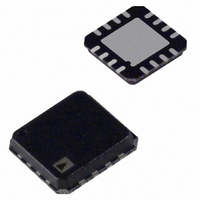
ADN2850BCP250 Analog Devices Inc, ADN2850BCP250 Datasheet - Page 16

ADN2850BCP250
Manufacturer Part Number
ADN2850BCP250
Description
IC DGTL RHEO DL 1024POS 16LFCSP
Manufacturer
Analog Devices Inc
Specifications of ADN2850BCP250
Taps
1024
Resistance (ohms)
250K
Number Of Circuits
2
Temperature Coefficient
35 ppm/°C Typical
Memory Type
Non-Volatile
Interface
4-Wire SPI Serial
Voltage - Supply
3 V ~ 5.5 V, ±2.25 V ~ 2.75 V
Operating Temperature
-40°C ~ 85°C
Mounting Type
Surface Mount
Package / Case
16-LFCSP
Resistance In Ohms
250K
Number Of Elements
2
# Of Taps
1024
Resistance (max)
250KOhm
Power Supply Requirement
Single/Dual
Interface Type
Serial (4-Wire/SPI)
Single Supply Voltage (typ)
5V
Dual Supply Voltage (typ)
±2.5V
Single Supply Voltage (min)
3V
Single Supply Voltage (max)
5.5V
Dual Supply Voltage (min)
±2.25V
Dual Supply Voltage (max)
±2.75V
Operating Temp Range
-40C to 85C
Operating Temperature Classification
Industrial
Mounting
Surface Mount
Pin Count
16
Lead Free Status / RoHS Status
Contains lead / RoHS non-compliant
For Use With
EVAL-ADN2850-25EBZ - BOARD EVALUATION FOR ADN2850-25
Lead Free Status / RoHS Status
Not Compliant, Contains lead / RoHS non-compliant
ADN2850
In Table 7, command bits are C0 to C3, address bits are A0 to A3, Data Bit D0 to Data Bit D9 are applicable to RDAC, and D0 to D15 are
applicable to EEMEM.
Table 7. 24-Bit Serial Data-Word
RDAC
EEMEM
Command instruction codes are defined in Table 8.
Table 8. Command Operation Truth Table
Command
Number
0
1
2
3
4
5
6
7
8
9
10
11
12
13
14
15
1
2
3
4
5
5
5
5
The SDO output shifts out the last 24 bits of data clocked into the serial register for daisy-chain operation. Exception: for any instruction following Instruction 9 or
Instruction 10, the selected internal register data is present in Data Byte 0 and Data Byte 1. The instructions following Instruction 9 and Instruction 10 must also be a
full 24-bit data-word to completely clock out the contents of the serial register.
The RDAC register is a volatile scratchpad register that is refreshed at power-on from the corresponding nonvolatile EEMEM register.
Execution of these operations takes place when the CS strobe returns to logic high.
Instruction 3 writes two data bytes (16 bits of data) to EEMEM. In the case of Address 0 and Address 1, only the last 10 bits are valid for wiper position setting.
The increment, decrement, and shift instructions ignore the contents of the shift register, Data Byte 0 and Data Byte 1.
4
5
5
5
5
5
MSB
C3
C3
B23
C3
0
0
0
0
0
0
0
0
1
1
1
1
1
1
1
1
C2
C2
C2
0
0
0
0
1
1
1
1
0
0
0
0
1
1
1
1
C1
C1
C1
0
0
1
1
0
0
1
1
0
0
1
1
0
0
1
1
C0
C0
Command Byte 0
Command Byte 0
0
A3
C0
0
1
0
1
0
1
0
1
0
1
0
1
0
1
0
1
0
A2
A3
X
0
0
A3
0
X
0
X
0
A3
0
0
0
X
0
X
0
A1
A2
X
0
0
A2
0
X
0
X
0
A2
0
0
0
X
0
X
A0
A0
1, 2, 3
A1
X
0
0
A1
0
X
0
X
0
A1
0
0
0
X
0
X
X
D15
B16
A0
X
A0
A0
A0
A0
X
A0
X
0
A0
A0
A0
A0
X
A0
X
X
D14
B15
X
X
X
X
D15
X
X
X
X
X
X
X
X
X
X
X
X
Rev. C | Page 16 of 28
Data Byte 1
X
D13
…
…
…
…
…
…
…
…
…
…
…
…
…
…
…
…
…
Data Byte 1
D9
X
X
X
X
X
X
X
X
X
X
D9
X
X
X
X
X
D12
B8
D8
X
X
X
D8
X
X
X
X
X
D8
X
X
X
X
X
X
X
D11
B7
D7
X
X
X
D7
X
X
X
X
X
X
X
D7
X
X
X
X
Data Byte 0
X
D10
…
…
…
…
…
…
…
…
…
…
…
…
…
…
…
…
…
D9
D9
B0
D0
X
X
X
D0
X
X
X
X
X
X
X
D0
X
X
X
X
D8
D8
Operation
NOP. Do nothing. See
Restore EEMEM (A0) contents to RDAC (A0)
register. See Table 16.
Store wiper setting. Store RDAC (A0) setting to
EEMEM (A0). See Table 15.
Store contents of Serial Register Data Byte 0 and
Serial Register Data Bytes 1 (total 16 bits) to
EEMEM (ADDR). See Table 18.
Decrement by 6 dB. Right-shift contents of RDAC
(A0) register, stop at all 0s.
Decrement all by 6 dB. Right-shift contents of all
RDAC registers, stop at all 0s.
Decrement contents of RDAC (A0) by 1, stop at
all 0s.
Decrement contents of all RDAC registers by 1,
stop at all 0s.
Reset. Refresh all RDACs with their corresponding
EEMEM previously stored values.
output in the next frame. See
Read RDAC wiper setting from SDO output in the
next frame. See Table 20.
Write contents of Serial Register Data Byte 0 and
Serial Register Data Byte 1 (total 10 bits) to RDAC
(A0). See Table 14.
Increment by 6 dB: Left-shift contents of RDAC (A0),
stop at all 1s. See
Increment all by 6 dB. Left-shift contents of all
RDAC registers, stop at all 1s.
Increment contents of RDAC (A0) by 1, stop at all
1s. See Table 15.
Increment contents of all RDAC registers by 1,
stop at all 1s.
Read contents of EEMEM (ADDR) from SDO
D7
D7
D6
D6
D5
D5
Data Byte 0
Table 17
D4
D4
Table 19
.
D3
D3
Table 19
D2
D2
.
D1
D1
D0
LSB
D0


