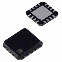
ADN2850BCP250 Analog Devices Inc, ADN2850BCP250 Datasheet - Page 7

ADN2850BCP250
Manufacturer Part Number
ADN2850BCP250
Description
IC DGTL RHEO DL 1024POS 16LFCSP
Manufacturer
Analog Devices Inc
Specifications of ADN2850BCP250
Taps
1024
Resistance (ohms)
250K
Number Of Circuits
2
Temperature Coefficient
35 ppm/°C Typical
Memory Type
Non-Volatile
Interface
4-Wire SPI Serial
Voltage - Supply
3 V ~ 5.5 V, ±2.25 V ~ 2.75 V
Operating Temperature
-40°C ~ 85°C
Mounting Type
Surface Mount
Package / Case
16-LFCSP
Resistance In Ohms
250K
Number Of Elements
2
# Of Taps
1024
Resistance (max)
250KOhm
Power Supply Requirement
Single/Dual
Interface Type
Serial (4-Wire/SPI)
Single Supply Voltage (typ)
5V
Dual Supply Voltage (typ)
±2.5V
Single Supply Voltage (min)
3V
Single Supply Voltage (max)
5.5V
Dual Supply Voltage (min)
±2.25V
Dual Supply Voltage (max)
±2.75V
Operating Temp Range
-40C to 85C
Operating Temperature Classification
Industrial
Mounting
Surface Mount
Pin Count
16
Lead Free Status / RoHS Status
Contains lead / RoHS non-compliant
For Use With
EVAL-ADN2850-25EBZ - BOARD EVALUATION FOR ADN2850-25
Lead Free Status / RoHS Status
Not Compliant, Contains lead / RoHS non-compliant
ABSOLUTE MAXIMUM RATINGS
T
Table 3.
Parameter
V
V
V
V
I
Digital Input and Output Voltage to GND
Operating Temperature Range
Maximum Junction Temperature (T
Storage Temperature Range
Lead Temperature, Soldering
Thermal Resistance
Package Power Dissipation
1
2
B
Maximum terminal current is bounded by the maximum current handling of
the switches, maximum power dissipation of the package, and maximum
applied voltage across any two of the A, B, and W terminals at a given
resistance.
Includes programming of nonvolatile memory.
DD
SS
DD
B
, I
A
, V
Pulsed
Continuous
Vapor Phase (60 sec)
Infrared (15 sec)
Junction-to-Ambient θ
Junction-to-Ambient θ
Junction-to-Case θ
W
= 25°C, unless otherwise noted.
to GND
to GND
to V
W
to GND
SS
1
JC
, TSSOP-16
JA
JA
,TSSOP-16
,LFSCP-16
2
J
max)
Rating
–0.3 V to +7 V
+0.3 V to −7 V
7 V
V
±20 mA
±2 mA
−0.3 V to V
−40°C to +85°C
150°C
−65°C to +150°C
215°C
220°C
150°C/W
35°C/W
28°C/W
(T
SS
J
max − T
− 0.3 V to V
DD
A
)/θ
+ 0.3 V
DD
JA
+ 0.3 V
Rev. C | Page 7 of 28
Stresses above those listed under Absolute Maximum Ratings
may cause permanent damage to the device. This is a stress
rating only; functional operation of the device at these or any
other conditions above those indicated in the operational
section of this specification is not implied. Exposure to absolute
maximum rating conditions for extended periods may affect
device reliability.
ESD CAUTION
ADN2850


