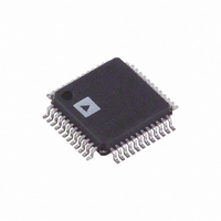
AD9772AASTZ Analog Devices Inc, AD9772AASTZ Datasheet - Page 10

AD9772AASTZ
Manufacturer Part Number
AD9772AASTZ
Description
IC DAC 14BIT 160MSPS 48-LQFP
Manufacturer
Analog Devices Inc
Series
TxDAC+®r
Datasheet
1.AD9772AASTZ.pdf
(40 pages)
Specifications of AD9772AASTZ
Data Interface
Parallel
Settling Time
11ns
Number Of Bits
14
Number Of Converters
1
Voltage Supply Source
Analog and Digital
Power Dissipation (max)
272mW
Operating Temperature
-40°C ~ 85°C
Mounting Type
Surface Mount
Package / Case
48-LQFP
Resolution (bits)
14bit
Sampling Rate
160MSPS
Input Channel Type
Parallel
Supply Voltage Range - Analog
3.1V To 3.5V
Supply Current
37mA
Digital Ic Case Style
QFP
Lead Free Status / RoHS Status
Lead free / RoHS Compliant
For Use With
AD9772A-EB - BOARD EVAL FOR AD9772A
Lead Free Status / RoHS Status
Lead free / RoHS Compliant, Lead free / RoHS Compliant
Available stocks
Company
Part Number
Manufacturer
Quantity
Price
Company:
Part Number:
AD9772AASTZ
Manufacturer:
TI
Quantity:
1 756
Company:
Part Number:
AD9772AASTZ
Manufacturer:
Analog Devices Inc
Quantity:
10 000
Part Number:
AD9772AASTZ
Manufacturer:
ADI/亚德诺
Quantity:
20 000
Company:
Part Number:
AD9772AASTZRL
Manufacturer:
Analog Devices Inc
Quantity:
10 000
Part Number:
AD9772AASTZRL
Manufacturer:
ADI/亚德诺
Quantity:
20 000
AD9772A
PIN CONFIGURATION AND FUNCTION DESCRIPTIONS
Table 8. Pin Function Descriptions
Pin No.
1, 2, 19, 20
3
4 to 15
16
17
18
23, 24
21, 22, 47, 48
25
26
27, 28
29
30
31
32
33
34
35
36
37, 41, 44
38
Mnemonic
DCOM
DB13
DB12 to DB1
DB0
MOD0
MOD1
NC
DVDD
PLLLOCK
RESET
DIV1, DIV0
CLK+
CLK−
CLKCOM
CLKVDD
PLLCOM
PLLVDD
LPF
SLEEP
ACOM
REFLO
Description
Digital Common.
Most Significant Data Bit (MSB).
Data Bit 1 to Data Bit 12.
Least Significant Data Bit (LSB).
Digital High-Pass Filter Response. Active high. This pin invokes the digital high-pass filter response (that is,
half-wave digital mixing mode). Note that quarter-wave digital mixing occurs if this pin and the MOD1 pin
are set high.
Zero-Stuffing Mode. Active high. This pin invokes zero-stuffing mode. Note that quarter-wave digital mixing
occurs if this pin and the MOD0 pin are set high.
No Connect. Leave open.
Digital Supply Voltage (3.1 V to 3.5 V).
Lock Signal of the Phase-Lock Loop. This pin provides the lock signal of the phase-lock loop when the PLL
clock multiplier is enabled, and provides the 1× clock output when the PLL clock multiplier is disabled. High
indicates that PLL is locked to the input clock. The maximum fanout is 1 (that is, <10 pF).
Internal Divider Reset. This pin can reset the internal driver to synchronize the internal 1× clock to the input
data and/or multiple AD9772A devices. The reset is initiated if this pin is momentarily brought high when
PLL is disabled.
PLL Prescaler Divide Ratio. DIV1 and DIV0 set the prescaler divide ratio of the PLL (refer to Table 10).
Noninverting Input to Differential Clock. Bias this pin to the midsupply (that is, CLKVDD/2).
Inverting Input to Differential Clock. Bias this pin to the midsupply (that is, CLKVDD/2).
Clock Input Common.
Clock Input Supply Voltage (3.1 V to 3.5 V).
Phase-Lock Loop Common.
Phase-Lock Loop (PLL) Supply Voltage (3.1 V to 3.5 V). To disable the PLL clock multiplier, connect PLLVDD to
PLLCOM.
PLL Loop Filter Node. This pin should be left as a no connect (open) unless the DAC update rate is less than
10 MSPS, in which case a series RC should be connected from LPF to PLLVDD as indicated in Figure 61.
Power-Down Control Input. Active high. When this pin is not used, connect it to ACOM.
Analog Common.
Reference Ground When Internal 1.2 V Reference Is Used. Connect this pin to AVDD to disable the internal
reference.
(MSB) DB13
NC = NO CONNECT
DCOM
DCOM
DB12
DB11
DB10
DB9
DB8
DB7
DB6
DB5
DB4
10
11
12
1
2
3
4
5
6
8
9
7
48 47 46 45 44
13 14 15 16 17 18 19 20 21 22 23 24
PIN 1
IDENTIFIER
Figure 6. Pin Configuration
Rev. C | Page 10 of 40
(Not to Scale)
AD9772A
TOP VIEW
43 42 41 40
39 38 37
36
35
34
33
32
31
30
29
28
27
26
25
SLEEP
LPF
PLLVDD
PLLCOM
CLKVDD
CLKCOM
CLK–
CLK+
DIV0
DIV1
RESET
PLLLOCK


