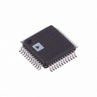
AD9772AASTZ Analog Devices Inc, AD9772AASTZ Datasheet - Page 7

AD9772AASTZ
Manufacturer Part Number
AD9772AASTZ
Description
IC DAC 14BIT 160MSPS 48-LQFP
Manufacturer
Analog Devices Inc
Series
TxDAC+®r
Datasheet
1.AD9772AASTZ.pdf
(40 pages)
Specifications of AD9772AASTZ
Data Interface
Parallel
Settling Time
11ns
Number Of Bits
14
Number Of Converters
1
Voltage Supply Source
Analog and Digital
Power Dissipation (max)
272mW
Operating Temperature
-40°C ~ 85°C
Mounting Type
Surface Mount
Package / Case
48-LQFP
Resolution (bits)
14bit
Sampling Rate
160MSPS
Input Channel Type
Parallel
Supply Voltage Range - Analog
3.1V To 3.5V
Supply Current
37mA
Digital Ic Case Style
QFP
Lead Free Status / RoHS Status
Lead free / RoHS Compliant
For Use With
AD9772A-EB - BOARD EVAL FOR AD9772A
Lead Free Status / RoHS Status
Lead free / RoHS Compliant, Lead free / RoHS Compliant
Available stocks
Company
Part Number
Manufacturer
Quantity
Price
Company:
Part Number:
AD9772AASTZ
Manufacturer:
TI
Quantity:
1 756
Company:
Part Number:
AD9772AASTZ
Manufacturer:
Analog Devices Inc
Quantity:
10 000
Part Number:
AD9772AASTZ
Manufacturer:
ADI/亚德诺
Quantity:
20 000
Company:
Part Number:
AD9772AASTZRL
Manufacturer:
Analog Devices Inc
Quantity:
10 000
Part Number:
AD9772AASTZRL
Manufacturer:
ADI/亚德诺
Quantity:
20 000
DIGITAL SPECIFICATIONS
T
Table 3.
Parameter
DIGITAL INPUTS
CLOCK INPUTS
PLL CLOCK ENABLED (SEE Figure 2)
PLL CLOCK DISABLED (SEE Figure 3)
1
DB0 TO DB13
CLK+ – CLK–
MOD0, MOD1, DIV0, DIV1, SLEEP, RESET have typical input currents of 15 μA.
MIN
Logic 1 Voltage
Logic 0 Voltage
Logic 1 Current
Logic 0 Current
Input Capacitance
Input Voltage Range
Common-Mode Voltage
Differential Voltage
Input Setup Time (t
Input Hold Time (t
Latch Pulse Width (t
Input Setup Time (t
Input Hold Time (t
Latch Pulse Width (t
CLK+/CLK− to PLLLOCK Delay (t
PLLLOCK (V
PLLLOCK (V
to T
T
T
T
T
T
T
T
T
T
T
A
A
A
A
A
A
A
A
A
A
I
I
OUTA
OUTB
= 25°C
= −40 to +85°C
= 25°C
= −40 to +85°C
= 25°C
= −40 to +85°C
= 25°C
= −40 to +85°C
= 25°C
= −40 to +85°C
OR
Figure 2. Timing Diagram—PLL Clock Multiplier Enabled
MAX
, AVDD = 3.3 V, CLKVDD = 3.3 V, PLLVDD = 0 V, DVDD = 3.3 V, I
OH
OL
), T
), T
1
A
A
= 25°C
= 25°C
H
H
)
)
S
S
t
LPW
LPW
)
)
S
), T
), T
A
A
t
PD
= 25°C
= 25°C
t
LPW
t
H
OD
)
0.025%
t
ST
0.025%
Rev. C | Page 7 of 40
DB0 TO DB13
CLK+ – CLK–
PLLLOCK
I
I
OUTFS
OUTA
OUTB
Min
2.1
−10
−10
0
0.75
0.5
1.5
2.1
1.3
1.6
1.5
−0.7
−0.4
3.3
3.7
1.5
1.9
1.8
3.0
Figure 3. Timing Diagram—PLL Clock Multiplier Disabled
OR
= 20 mA, unless otherwise noted.
t
S
Typ
3
0
5
1.5
1.5
t
OD
t
PD
t
t
LPW
H
Max
0.9
+10
+10
3
2.25
2.8
3.3
0.3
0.025%
t
ST
AD9772A
Unit
V
V
μA
μA
pF
V
V
V
ns
ns
ns
ns
ns
ns
ns
ns
ns
ns
ns
ns
V
V
0.025%


