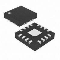
MAX5550ETE+ Maxim Integrated Products, MAX5550ETE+ Datasheet

MAX5550ETE+
Specifications of MAX5550ETE+
Related parts for MAX5550ETE+
MAX5550ETE+ Summary of contents
Page 1
... PIN Diode Biasing RF Attenuator Control VCO Tuning SPI is a trademark of Motorola, Inc. Pin Configuration appears at end of data sheet. ________________________________________________________________ Maxim Integrated Products For pricing, delivery, and ordering information, please contact Maxim/Dallas Direct! at 1-888-629-4642, or visit Maxim’s website at www.maxim-ic.com. High-Output-Current DAC ♦ Pin-Selectable I ♦ ...
Page 2
Dual, 10-Bit, Programmable, 30mA High-Output-Current DAC ABSOLUTE MAXIMUM RATINGS V to GND .............................................................-0.3V to +6V DD OUTA, OUTB to GND .................................-0. CS/AO, DOUT/AI, SPI/I2C, FSADJA, REFIN, FSADJB to GND ......................................-0. SCLK/SCL, DIN/SDA ................................................-0.3V to +6V Continuous ...
Page 3
Dual, 10-Bit, Programmable, 30mA ELECTRICAL CHARACTERISTICS (continued +2.7V to +5.25V, GND = -40°C to +85°C, unless otherwise noted. Typical values are at V SCLK/SCL A PARAMETER SYMBOL Digital-to-Analog Glitch Impulse ...
Page 4
Dual, 10-Bit, Programmable, 30mA High-Output-Current DAC ELECTRICAL CHARACTERISTICS (continued +2.7V to +5.25V, GND = REFIN -40°C to +85°C, unless otherwise noted. Typical values are at V SCLK/SCL A PARAMETER SYMBOL ...
Page 5
Dual, 10-Bit, Programmable, 30mA (V = +3.0V, GND = +1.25V, internal reference REFIN INL vs. CODE 2.0 1.5 1.0 0.5 0 -0.5 -1.0 -1.5 -2.0 0 128 256 384 512 640 768 896 1024 CODE ...
Page 6
Dual, 10-Bit, Programmable, 30mA High-Output-Current DAC (V = +3.0V, GND = +1.25V, internal reference REFIN GLITCH IMPULSE 40ns/div SHUTDOWN CURRENT vs. TEMPERATURE 620 NO LOAD, CODE = 0x00 520 420 V ...
Page 7
Dual, 10-Bit, Programmable, 30mA (V = +3.0V, GND = +1.25V, internal reference REFIN SUPPLY CURRENT vs. SUPPLY VOLTAGE 2.80 NO LOAD, CODE = 0x00 2.75 INTERNAL REFERENCE 2.70 2.65 EXTERNAL REFERENCE 2.60 2.5 3.0 3.5 ...
Page 8
Dual, 10-Bit, Programmable, 30mA High-Output-Current DAC PIN NAME SCLK/SC 1 Serial Clock Input. Connect SCL DIN/SDA Serial Data Input. Connect SDA to V Chip-Select Input in SPI Mode/Address Select CS/ GND to ...
Page 9
Dual, 10-Bit, Programmable, 30mA Compatibility (SPI/ The MAX5550 is compatible with existing I (Figure 2). SCL and SDA are high-impedance inputs; SDA has an open-drain output that pulls the data line low during the ninth clock pulse. ...
Page 10
Dual, 10-Bit, Programmable, 30mA High-Output-Current DAC S t RDA SDA t FDA t HD:DAT t t SU:STA HD:STA SCL t RCL t HIGH 2 Figure Serial-Interface Timing Diagram Early STOP Conditions The MAX5550 recognizes a STOP condition ...
Page 11
Dual, 10-Bit, Programmable, 30mA S SDA SCL Figure 5. Acknowledge Condition Table 3. Write Operation S T ADDRESS A BYTE Master SDA Slave SDA *Read operation not ...
Page 12
Dual, 10-Bit, Programmable, 30mA High-Output-Current DAC CSO CSS SCLK MSB DIN t CSE DOUT Figure 6. SPI-Interface Timing Diagram CS SCLK DIN Figure 7. SPI-Interface Format Applications ...
Page 13
Dual, 10-Bit, Programmable, 30mA Table 4. Command Summary SERIAL DATA INPUT ...
Page 14
Dual, 10-Bit, Programmable, 30mA High-Output-Current DAC DIN(0) CONTROLLER SCLK DEVICE CS DIN(1) SCLK CS DIN(2) SCLK CS Figure 8. Daisy-Chain Configuration Power Sequencing Ensure that the voltage applied to REFIN does not exceed V at any time. If proper power ...
Page 15
... Maxim cannot assume responsibility for use of any circuitry other than circuitry entirely embodied in a Maxim product. No circuit patent licenses are implied. Maxim reserves the right to change the circuitry and specifications without notice at any time. Maxim Integrated Products, 120 San Gabriel Drive, Sunnyvale, CA 94086 408-737-7600 _____________________ 1 © 2006 Maxim Integrated Products ...


