AD5763CSUZ Analog Devices Inc, AD5763CSUZ Datasheet - Page 10
AD5763CSUZ
Manufacturer Part Number
AD5763CSUZ
Description
DAC 16BIT DUAL 5V 2LSB 32-TQFP
Manufacturer
Analog Devices Inc
Datasheet
1.AD5763CSUZ.pdf
(28 pages)
Specifications of AD5763CSUZ
Data Interface
Serial
Design Resources
High Accuracy, Bipolar Voltage Output Digital-to-Analog Conversion Using AD5763 (CN0074)
Settling Time
8µs
Number Of Bits
16
Number Of Converters
2
Voltage Supply Source
Dual ±
Power Dissipation (max)
45mW
Operating Temperature
-40°C ~ 105°C
Mounting Type
Surface Mount
Package / Case
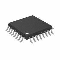
32-TQFP, 32-VQFP
Resolution (bits)
16bit
Input Channel Type
Serial
Supply Voltage Range - Analogue
4.75V To 5.25V
Supply Voltage Range - Digital
2.7V To 5.25V
Supply
RoHS Compliant
Lead Free Status / RoHS Status
Lead free / RoHS Compliant
Available stocks
Company
Part Number
Manufacturer
Quantity
Price
Company:

Part Number:
AD5763CSUZ
Manufacturer:
Analog Devices Inc
Quantity:
135
Company:
Part Number:
AD5763CSUZ
Manufacturer:
Analog Devices Inc
Quantity:
10 000
Company:
Part Number:
AD5763CSUZ-REEL7
Manufacturer:
Analog Devices Inc
Quantity:
10 000


AD5763
PIN CONFIGURATION AND FUNCTION DESCRIPTIONS
Table 6. Pin Function Descriptions
Pin No.
1
2
3
4
5
6
7, 8
9
10
11
12
13, 31
14
15, 30
16
17, 18, 23, 24, 27
19
20
21
1
Mnemonic
SYNC
SCLK
SDIN
SDO
CLR
LDAC
D0, D1
RSTOUT
RSTIN
DGND
DV
AV
PGND
AV
ISCC
NC
VOUTB
AGNDB
AGNDA
DD
SS
CC
Description
Active Low Input. This pin is the frame synchronization signal for the serial interface. While SYNC is
low, data is transferred in on the falling edge of SCLK.
Serial Clock Input. Data is clocked into the shift register on the falling edge of SCLK. This pin
operates at clock speeds up to 30 MHz.
Serial Data Input. Data must be valid on the falling edge of SCLK.
Serial Data Output. Used to clock data from the serial register in daisy-chain or readback mode.
Negative Edge Triggered Input. Asserting this pin sets the DAC registers to 0x0000.
Load DAC. Logic input. This pin is used to update the DAC registers and consequently the analog
outputs. When LDAC is tied permanently low, the addressed DAC register is updated on the rising
edge of SYNC. If LDAC is held high during the write cycle, the DAC input register is updated but the
output update is held off until the falling edge of LDAC. In this mode, all analog outputs can be
updated simultaneously on the falling edge of LDAC. The LDAC pin must not be left unconnected.
D0 and D1 form a digital I/O port. The user can set up these pins as inputs or outputs that are confi-
gurable and readable over the serial interface. When configured as inputs, these pins have weak
internal pull-ups to DV
Reset Logic Output. This pin is the output from the on-chip voltage monitor used in the reset
circuit. If desired, it can be used to control other system components.
Reset Logic Input. This input allows external access to the internal reset logic. Applying a Logic 0 to
this input clamps the DAC outputs to 0 V. In normal operation, RSTIN should be tied to Logic 1.
Register values remain unchanged.
Digital Ground Pin.
Digital Supply Pin. The voltage ranges from 2.7 V to 5.25 V.
Positive Analog Supply Pins. The voltage ranges from 4.75 V to 5.25 V.
Ground Reference Point for Analog Circuitry.
Negative Analog Supply Pins. The voltage ranges from –5.25 V to –4.75 V.
This pin is used in association with an optional external resistor connected to AGND and programs
the short-circuit current of the output amplifiers. See the Design Features section for further details.
No Connect.
Analog Output Voltage of DAC B. Buffered output with a nominal full-scale output range of ±4.096 V. The
output amplifier is capable of directly driving a 5 kΩ, 200 pF load.
Ground Reference Pin for the DAC B Output Amplifier.
Ground Reference Pin for the DAC A Output Amplifier.
SYNC
LDAC
SCLK
SDIN
SDO
CLR
D0
D1
1
8
32
9
Figure 6. Pin Configuration
NC = NO CONNECT
Rev. A | Page 10 of 28
PIN 1
INDICATOR
CC
(Not to scale)
. When programmed as outputs, D0 and D1 are referenced by DV
AD5763
TOP VIEW
25
16
24
17
NC
NC
VOUTA
AGNDA
AGNDB
VOUTB
NC
NC
1
CC
and DGND.
Related parts for AD5763CSUZ
Image
Part Number
Description
Manufacturer
Datasheet
Request
R

Part Number:
Description:
±1.7g Dual-Axis IMEMS Accelerometer Evaluation Board
Manufacturer:
Analog Devices Inc
Datasheet:

Part Number:
Description:
Inertial Sensor Evaluation System
Manufacturer:
Analog Devices Inc
Datasheet:
Part Number:
Description:
Manufacturer:
Analog Devices Inc
Datasheet:
Part Number:
Description:
Manufacturer:
Analog Devices Inc
Datasheet:
Part Number:
Description:
Manufacturer:
Analog Devices Inc
Datasheet:
Part Number:
Description:
Manufacturer:
Analog Devices Inc
Datasheet:
Part Number:
Description:
Manufacturer:
Analog Devices Inc
Datasheet:
Part Number:
Description:
Manufacturer:
Analog Devices Inc
Datasheet:
Part Number:
Description:
Manufacturer:
Analog Devices Inc
Datasheet:
Part Number:
Description:
Manufacturer:
Analog Devices Inc
Datasheet:
Part Number:
Description:
Manufacturer:
Analog Devices Inc
Datasheet:
Part Number:
Description:
Manufacturer:
Analog Devices Inc
Datasheet:
Part Number:
Description:
Manufacturer:
Analog Devices Inc
Datasheet: