AD5763CSUZ Analog Devices Inc, AD5763CSUZ Datasheet - Page 6
AD5763CSUZ
Manufacturer Part Number
AD5763CSUZ
Description
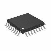
DAC 16BIT DUAL 5V 2LSB 32-TQFP
Manufacturer
Analog Devices Inc
Datasheet
1.AD5763CSUZ.pdf
(28 pages)
Specifications of AD5763CSUZ
Data Interface
Serial
Design Resources
High Accuracy, Bipolar Voltage Output Digital-to-Analog Conversion Using AD5763 (CN0074)
Settling Time
8µs
Number Of Bits
16
Number Of Converters
2
Voltage Supply Source
Dual ±
Power Dissipation (max)
45mW
Operating Temperature
-40°C ~ 105°C
Mounting Type
Surface Mount
Package / Case
32-TQFP, 32-VQFP
Resolution (bits)
16bit
Input Channel Type
Serial
Supply Voltage Range - Analogue
4.75V To 5.25V
Supply Voltage Range - Digital
2.7V To 5.25V
Supply
RoHS Compliant
Lead Free Status / RoHS Status
Lead free / RoHS Compliant
Available stocks
Company
Part Number
Manufacturer
Quantity
Price
Company:

Part Number:
AD5763CSUZ
Manufacturer:
Analog Devices Inc
Quantity:
135
Company:
Part Number:
AD5763CSUZ
Manufacturer:
Analog Devices Inc
Quantity:
10 000
Company:
Part Number:
AD5763CSUZ-REEL7
Manufacturer:
Analog Devices Inc
Quantity:
10 000


AD5763
TIMING CHARACTERISTICS
AV
DV
Table 4.
Parameter
t
t
t
t
t
t
t
t
t
t
t
t
t
t
t
t
t
t
1
2
3
4
5
6
1
2
3
4
5
6
7
8
9
10
11
12
13
14
15
16
17
18
Guaranteed by design and characterization; not production tested.
All input signals are specified with t
See Figure 2, Figure 3, and Figure 4.
Standalone mode only.
Measured with the load circuit of Figure 5.
Daisy-chain mode only.
4
5, 6
DD
CC
= 4.75 V to 5.25 V, AV
= 2.7 V to 5.25 V, R
1, 2, 3
LOAD
SS
Limit at T
33
13
13
13
13
90
2
5
1.7
480
10
500
10
10
2
25
13
2
170
= 5 kΩ, C
= −5.25 V to −4.75 V, AGNDx = DGND = REFGND = PGND = 0 V, REFA = REFB = 2.048 V,
R
= t
F
= 5 ns (10% to 90% of DV
MIN
LOAD
, T
= 200 pF. All specifications T
MAX
CC
) and timed from a voltage level of 1.2 V.
Unit
ns min
ns min
ns min
ns min
ns min
ns min
ns min
ns min
μs min
ns min
ns min
ns max
μs max
ns min
μs max
ns max
ns min
μs max
ns min
Rev. A | Page 6 of 28
Description
SCLK cycle time
SCLK high time
SCLK low time
SYNC falling edge to SCLK falling edge setup time
24
Minimum SYNC high time
Data setup time
Data hold time
SYNC rising edge to LDAC falling edge (all DACs updated)
SYNC rising edge to LDAC falling edge (single DAC updated)
LDAC pulse width low
LDAC falling edge to DAC output response time
DAC output settling time
CLR pulse width low
CLR pulse activation time
SCLK rising edge to SDO valid
SYNC rising edge to SCLK falling edge
SYNC rising edge to DAC output response time (LDAC= 0)
LDAC falling edge to SYNC rising edge
th
MIN
SCLK falling edge to SYNC rising edge
to T
MAX
, unless otherwise noted.
Related parts for AD5763CSUZ
Image
Part Number
Description
Manufacturer
Datasheet
Request
R

Part Number:
Description:
±1.7g Dual-Axis IMEMS Accelerometer Evaluation Board
Manufacturer:
Analog Devices Inc
Datasheet:

Part Number:
Description:
Inertial Sensor Evaluation System
Manufacturer:
Analog Devices Inc
Datasheet:
Part Number:
Description:
Manufacturer:
Analog Devices Inc
Datasheet:
Part Number:
Description:
Manufacturer:
Analog Devices Inc
Datasheet:
Part Number:
Description:
Manufacturer:
Analog Devices Inc
Datasheet:
Part Number:
Description:
Manufacturer:
Analog Devices Inc
Datasheet:
Part Number:
Description:
Manufacturer:
Analog Devices Inc
Datasheet:
Part Number:
Description:
Manufacturer:
Analog Devices Inc
Datasheet:
Part Number:
Description:
Manufacturer:
Analog Devices Inc
Datasheet:
Part Number:
Description:
Manufacturer:
Analog Devices Inc
Datasheet:
Part Number:
Description:
Manufacturer:
Analog Devices Inc
Datasheet:
Part Number:
Description:
Manufacturer:
Analog Devices Inc
Datasheet:
Part Number:
Description:
Manufacturer:
Analog Devices Inc
Datasheet: