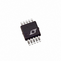
LTC2634IMSE-HZ12#TRPBF Linear Technology, LTC2634IMSE-HZ12#TRPBF Datasheet - Page 16

LTC2634IMSE-HZ12#TRPBF
Manufacturer Part Number
LTC2634IMSE-HZ12#TRPBF
Description
IC DAC 12BIT QUAD 2.5V 10-MSOP
Manufacturer
Linear Technology
Datasheet
1.LTC2634IMSE-LZ10PBF.pdf
(30 pages)
Specifications of LTC2634IMSE-HZ12#TRPBF
Settling Time
4.2µs
Number Of Bits
12
Data Interface
MICROWIRE™, Serial, SPI™
Number Of Converters
4
Voltage Supply Source
Single Supply
Power Dissipation (max)
1.8mW
Operating Temperature
-40°C ~ 85°C
Mounting Type
Surface Mount
Package / Case
10-MSOP Exposed Pad, 10-HMSOP, 10-eMSOP
Lead Free Status / RoHS Status
Lead free / RoHS Compliant
Available stocks
Company
Part Number
Manufacturer
Quantity
Price
pin Functions
LTC2634
V
Analog Voltage Outputs.
LDAC (Pin 3, QFN Only): Asynchronous DAC Update
Pin. If CS/LD is high, a falling edge on LDAC immediately
updates the DAC registers with the contents of the input
registers (similar to a software update). If CS/LD is low
when LDAC goes low, the DAC registers are updated after
CS/LD returns high. A low on the LDAC pin powers up
the DACs. A software power-down command is ignored
if LDAC is low.
CS/LD (Pin 4/Pin 4): Serial Interface Chip Select/Load
Input. When CS/LD is low, SCK is enabled for shifting
data on SDI into the 32-bit shift register. When CS/LD is
taken high, SCK is disabled and the specified command
(see Table 1) is executed.
SCK (Pin 5/Pin 5): Serial Interface Clock Input. CMOS
and TTL compatible.
DNC (Pins 6, 15, QFN Only): Do not connect these
pins.
SDO (Pin 7, QFN Only): Serial Interface Data Output. The
serial output of the 32-bit shift register appears at the SDO
pin. The data transferred to the device via the SDI pin is
delayed 32 SCK rising edges before being output at the
next falling edge. This pin is used for daisy-chain opera-
tion, it is always driven and never goes high impedance,
even when CS/LD is high. See the Daisy-Chain Operation
section.
OUTA
to V
OUTD
(Pins 1-2, 11-12/Pins 2-3, 8-9): DAC
(QFN/MSOP)
SDI (Pin 8/Pin 6): Serial Interface Data Input. Data on
SDI is clocked into the DAC on the rising edge of SCK.
The LTC2634 accepts input word lengths of either 24 or
32 bits.
CLR (Pin 9, QFN Only): Asynchronous Clear Input. A
logic low at this level-triggered input clears all registers
and causes the DAC voltage output to reset to zero
(LTC2634-Z) or mid-scale (LTC2634-MI/-MX). CMOS and
TTL compatible.
REF (Pin 10/Pin 7): Reference Voltage Input or Output.
When external reference mode is selected, REF is an input
(1V ≤ V
full-scale DAC output voltage. When internal reference
is selected, the 10ppm/°C 1.25V (LTC2634-L) or 2.048V
(LTC2634-H) internal reference (half full-scale) is available
at REF. This output may be bypassed to GND with up to
10µF and must be buffered when driving external DC load
current.
REFLO (Pin 13, QFN only): Reference Low Pin. The voltage
at this pin sets the zero-scale voltage of all DACs. This pin
must be tied to GND.
GND (Pin 14/Pin 10): Ground.
V
5.5V (LTC2634-L) or 4.5V ≤ V
Bypass to GND with a 0.1µF capacitor.
Exposed Pad (Pin 17/Pin 11): Ground. Must be soldered
to PCB ground.
CC
(Pin 16/Pin 1): Supply Voltage Input. 2.7V ≤ V
REF
≤ V
CC
) where the voltage supplied sets the
CC
≤ 5.5V (LTC2634-H).
CC
2634fc
≤


