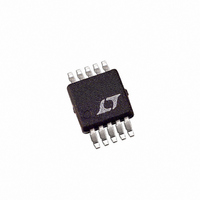
LTC2634IMSE-HZ12#TRPBF Linear Technology, LTC2634IMSE-HZ12#TRPBF Datasheet - Page 21

LTC2634IMSE-HZ12#TRPBF
Manufacturer Part Number
LTC2634IMSE-HZ12#TRPBF
Description
IC DAC 12BIT QUAD 2.5V 10-MSOP
Manufacturer
Linear Technology
Datasheet
1.LTC2634IMSE-LZ10PBF.pdf
(30 pages)
Specifications of LTC2634IMSE-HZ12#TRPBF
Settling Time
4.2µs
Number Of Bits
12
Data Interface
MICROWIRE™, Serial, SPI™
Number Of Converters
4
Voltage Supply Source
Single Supply
Power Dissipation (max)
1.8mW
Operating Temperature
-40°C ~ 85°C
Mounting Type
Surface Mount
Package / Case
10-MSOP Exposed Pad, 10-HMSOP, 10-eMSOP
Lead Free Status / RoHS Status
Lead free / RoHS Compliant
Available stocks
Company
Part Number
Manufacturer
Quantity
Price
operation
While the minimum input sequence is 24 bits, it may
optionally be extended to 32 bits to accommodate micro-
processors that have a minimum word width of 16 bits
(2 bytes). To use the 32-bit width, 8 don’t care bits
must be transferred to the device first, followed by the
24-bit sequence described. Figure 3b shows the 32-bit
sequence.
The 16-bit data word is ignored for all commands that do
not include a write operation.
Daisy-Chain Operation (QFN Package)
The serial output of the shift register appears at the SDO
pin on the QFN package. Data transferred to the device
from the SDI input is delayed 32 SCK rising edges before
being output at the next SCK falling edge, therefore, daisy
chaining multiple LTC2634 DACs requires 32-bit data
write cycles.
The SDO output can be used to facilitate control of multiple
serial devices from a single 3-wire serial port (i.e., SCK,
SDI and CS/LD). Such a “daisy-chain” series is configured
by connecting SDO of each upstream device to SDI of the
next device in the chain. The shift registers of the devices
are thus connected in series, effectively forming a single
input shift register which extends through the entire chain.
Because of this, the devices can be addressed and controlled
individually by simply concatenating their input words;
the first instruction addresses the last device in the chain
and so forth. The SCK and CS/LD signals are common to
all devices in the series. Figure 5 shows a block diagram
for daisy-chain operation.
In use, CS/LD is first taken low. Then the concatenated
input data is transferred to the chain, using SDI of the
first device as the data input. When the data transfer is
complete, CS/LD is taken high, completing the instruction
sequence for all devices simultaneously. A single device
can be controlled by using the no-operation command
(1111) for the other devices in the chain.
Reference Modes
For applications where an accurate external reference is
either not available, or not desirable due to limited space,
the LTC2634 has a low noise, user-selectable, integrated
reference. The integrated reference voltage is internally
amplified by 2x to provide the full-scale DAC output volt-
age range. The LTC2634-LMI/LTC2634-LMX/LTC2634-LZ
provides a full-scale DAC output of 2.5V. The LTC2634-
HMI/LTC2634-HMX/LTC2634-HZ provides a full-scale
DAC output of 4.096V. The internal reference can be
useful in applications where the supply voltage is poorly
regulated. Internal Reference mode can be selected by
using command 0110b, and is the power-on default for
LTC2634-HZ/LTC2634-LZ, as well as for LTC2634-HMI/
LTC2634-LMI.
The 10ppm/°C, 1.25V (LTC2634-LMI/LTC2634-LMX/
LTC2634-LZ) or 2.048V (LTC2634-HMI/LTC2634-HMX/
LTC2634-HZ) internal reference is available at the REF pin.
Adding bypass capacitance to the REF pin will improve
noise performance; 0.1µF is recommended, and up to 10µF
can be driven without oscillation. The REF output must be
buffered when driving an external DC load current.
Alternatively, the DAC can operate in external reference
mode using command 0111b. In this mode, an input voltage
supplied externally to the REF pin provides the reference
(1V ≤ V
external reference voltage supplied sets the full-scale DAC
output voltage. External reference mode is the power-on
default for LTC2634-HMX/LTC2634-LMX.
The reference mode of LTC2634-HZ/LTC2634-LZ/
LTC2634-HMI/LTC2634-LMI (internal reference power-on
default), can be changed by software command after power
up. The same is true for LTC2634-HMX/-LMX (external
reference power-on default).
The LTC2634’s QFN package offers a REFLO pin for the
negative reference. REFLO must be connected to GND.
REF
≤ V
CC
) and the supply current is reduced. The
LTC2634
2634fc


