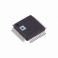
AD9709ASTZ Analog Devices Inc, AD9709ASTZ Datasheet - Page 17

AD9709ASTZ
Manufacturer Part Number
AD9709ASTZ
Description
IC DAC 8BIT DUAL 125MSPS 48-LQFP
Manufacturer
Analog Devices Inc
Series
TxDAC+®r
Datasheet
1.AD9709ASTZRL.pdf
(32 pages)
Specifications of AD9709ASTZ
Data Interface
Parallel
Settling Time
35ns
Number Of Bits
8
Number Of Converters
2
Voltage Supply Source
Analog and Digital
Power Dissipation (max)
450mW
Operating Temperature
-40°C ~ 85°C
Mounting Type
Surface Mount
Package / Case
48-LQFP
Resolution (bits)
8bit
Sampling Rate
125MSPS
Input Channel Type
Parallel
Supply Voltage Range - Analog
3V To 5.5V
Supply Voltage Range - Digital
2.7V To 5.5V
Lead Free Status / RoHS Status
Lead free / RoHS Compliant
For Use With
AD9709-EBZ - BOARD EVAL FOR AD9709
Lead Free Status / RoHS Status
Lead free / RoHS Compliant, Lead free / RoHS Compliant
Available stocks
Company
Part Number
Manufacturer
Quantity
Price
Company:
Part Number:
AD9709ASTZ
Manufacturer:
ADI
Quantity:
19
Company:
Part Number:
AD9709ASTZ
Manufacturer:
AD
Quantity:
170
Company:
Part Number:
AD9709ASTZ
Manufacturer:
Analog Devices Inc
Quantity:
10 000
Part Number:
AD9709ASTZ
Manufacturer:
ADI/亚德诺
Quantity:
20 000
Company:
Part Number:
AD9709ASTZRL
Manufacturer:
NECTOKIN
Quantity:
4 309
Company:
Part Number:
AD9709ASTZRL
Manufacturer:
Analog Devices Inc
Quantity:
10 000
Digital signal paths should be kept short, and run lengths should be
matched to avoid propagation delay mismatch. The insertion of
a low value (that is, 20 Ω to 100 Ω) resistor network between
the AD9709 digital inputs and driver outputs may be helpful in
reducing any overshooting and ringing at the digital inputs that
contribute to digital feedthrough. For longer board traces and
high data update rates, stripline techniques with proper
impedance and termination resistors should be considered to
maintain “clean” digital inputs.
The external clock driver circuitry provides the AD9709 with a
low-jitter clock input meeting the minimum and maximum logic
levels while providing fast edges. Fast clock edges help minimize
jitter manifesting itself as phase noise on a reconstructed waveform.
Therefore, the clock input should be driven by the fastest logic
family suitable for the application.
Note that the clock input can also be driven via a sine wave, which
is centered around the digital threshold (that is, DVDDx/2) and
meets the minimum and maximum logic threshold. This typically
results in a slight degradation in the phase noise, which becomes
more noticeable at higher sampling rates and output frequencies.
In addition, at higher sampling rates, the 20% tolerance of the
digital logic threshold should be considered because it affects
the effective clock duty cycle and, subsequently, cut into the
required data setup and hold times.
Rev. B | Page 17 of 32
Input Clock and Data Timing Relationship
SNR in a DAC is dependent on the relationship between the
position of the clock edges and the point in time at which the
input data changes. The AD9709 is rising-edge triggered and
therefore exhibits SNR sensitivity when the data transition is
close to this edge. In general, the goal when applying the AD9709 is
to make the data transition close to the falling clock edge. This
becomes more important as the sample rate increases. Figure 32
shows the relationship of SNR to clock/data placement.
Figure 32. SNR vs. Clock Placement @ f
60
50
40
30
20
10
0
–4
–3
TIME OF DATA CHANGE RELATIVE TO
–2
RISING CLOCK EDGE (ns)
–1
0
OUT
= 20 MHz and f
1
2
CLK
3
AD9709
= 125 MSPS
4


