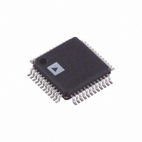
AD9709ASTZ Analog Devices Inc, AD9709ASTZ Datasheet - Page 20

AD9709ASTZ
Manufacturer Part Number
AD9709ASTZ
Description
IC DAC 8BIT DUAL 125MSPS 48-LQFP
Manufacturer
Analog Devices Inc
Series
TxDAC+®r
Datasheet
1.AD9709ASTZRL.pdf
(32 pages)
Specifications of AD9709ASTZ
Data Interface
Parallel
Settling Time
35ns
Number Of Bits
8
Number Of Converters
2
Voltage Supply Source
Analog and Digital
Power Dissipation (max)
450mW
Operating Temperature
-40°C ~ 85°C
Mounting Type
Surface Mount
Package / Case
48-LQFP
Resolution (bits)
8bit
Sampling Rate
125MSPS
Input Channel Type
Parallel
Supply Voltage Range - Analog
3V To 5.5V
Supply Voltage Range - Digital
2.7V To 5.5V
Lead Free Status / RoHS Status
Lead free / RoHS Compliant
For Use With
AD9709-EBZ - BOARD EVAL FOR AD9709
Lead Free Status / RoHS Status
Lead free / RoHS Compliant, Lead free / RoHS Compliant
Available stocks
Company
Part Number
Manufacturer
Quantity
Price
Company:
Part Number:
AD9709ASTZ
Manufacturer:
ADI
Quantity:
19
Company:
Part Number:
AD9709ASTZ
Manufacturer:
AD
Quantity:
170
Company:
Part Number:
AD9709ASTZ
Manufacturer:
Analog Devices Inc
Quantity:
10 000
Part Number:
AD9709ASTZ
Manufacturer:
ADI/亚德诺
Quantity:
20 000
Company:
Part Number:
AD9709ASTZRL
Manufacturer:
NECTOKIN
Quantity:
4 309
Company:
Part Number:
AD9709ASTZRL
Manufacturer:
Analog Devices Inc
Quantity:
10 000
AD9709
SINGLE-ENDED, UNBUFFERED VOLTAGE OUTPUT
Figure 39 shows the AD9709 configured to provide a unipolar
output range of approximately 0 V to 0.5 V for a doubly terminated
50 Ω cable, because the nominal full-scale current, I
flows through the equivalent R
represents the equivalent load resistance seen by I
The unused output (I
ACOM or via a matching R
R
adhered to. One additional consideration in this mode is the
INL (see the Analog Outputs section). For optimum INL
performance, the single-ended, buffered voltage output
configuration is suggested.
SINGLE-ENDED, BUFFERED VOLTAGE OUTPUT
CONFIGURATION
Figure 40 shows a buffered single-ended output configuration
in which the U1 op amp performs an I-V conversion on the
AD9709 output current. U1 maintains I
virtual ground, thus minimizing the nonlinear output
impedance effect on the INL performance of the DAC, as
discussed in the Analog Outputs section. Although this single-
ended configuration typically provides the best dc linearity
performance, its ac distortion performance at higher DAC
update rates may be limited by the slewing capabilities of U1.
U1 provides a negative unipolar output voltage, and its full-
scale output voltage is simply the product of R
full-scale output should be set within U1’s voltage output swing
capabilities by scaling I
distortion performance may result with a reduced I
the signal current U1 has to sink will be subsequently reduced.
LOAD
AD9709
can be selected as long as the positive compliance range is
AD9709
I
I
OUTA
OUTB
Figure 39. 0 V to 0.5 V Unbuffered Voltage Output
I
I
OUTA
OUTB
Figure 40. Unipolar Buffered Voltage Output
I
OUTFS
I
OUTFS
OUTA
OUTFS
= 10mA
25Ω
= 20mA
or I
200Ω
LOAD
and/or R
LOAD
OUTB
. Different values of I
50Ω
) can be connected directly to
of 25 Ω. In this case, R
FB
C
200Ω
R
U1
. An improvement in ac
OPT
FB
OUTA
V
OUTA
(or I
FB
V
OUT
50Ω
= 0V TO 0.5V
and I
OUTB
OUTFS
OUTA
= I
OUTFS
OUTFS
OUTFS
) at a
, of 20 mA
or I
OUTFS
LOAD
because
OUTB
× R
and
. The
FB
Rev. B | Page 20 of 32
.
POWER AND GROUNDING CONSIDERATIONS
Power Supply Rejection
Many applications seek high speed and high performance under
less than ideal operating conditions. In these applications, the
implementation and construction of the printed circuit board is
as important as the circuit design. Proper RF techniques must
be used for device selection, placement, and routing as well as
power supply bypassing and grounding to ensure optimum
performance. Figure 52 and Figure 53 illustrate the recommended
circuit board layout, including ground, power, and signal
input/output.
One factor that can measurably affect system performance is
the ability of the DAC output to reject dc variations or ac noise
superimposed on the analog or digital dc power distribution.
This is referred to as the power supply rejection ratio (PSRR).
For dc variations of the power supply, the resulting performance
of the DAC directly corresponds to a gain error associated with
the DAC’s full-scale current, I
is common in applications where the power distribution is
generated by a switching power supply. Typically, switching
power supply noise occurs over the spectrum from tens of
kilohertz to several megahertz. The PSRR vs. frequency of the
AD9709 AVDD supply over this frequency range is shown in
Figure 41.
Note that the data in Figure 41 is given in terms of current out
vs. voltage in. Noise on the analog power supply has the effect
of modulating the internal current sources and therefore the
output current. The voltage noise on AVDD, therefore, is added
in a nonlinear manner to the desired I
dependent, thus producing mixing effects that can modulate
low frequency power supply noise to higher frequencies. Worst-
case PSRR for either one of the differential DAC outputs occurs
when the full-scale current is directed toward that output. As a
result, the PSRR measurement in Figure 41 represents a worst-
case condition in which the digital inputs remain static and the
full-scale output current of 20 mA is directed to the DAC
output being measured.
90
85
80
75
70
Figure 41. AVDD Power Supply Rejection Ratio vs. Frequency
0.2
0.3
0.4
0.5
FREQUENCY (MHz)
0.6
OUTFS
. AC noise on the dc supplies
0.7
OUT
0.8
. PSRR is very code
0.9
1.0
1.1


