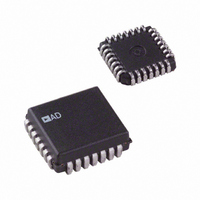
AD7846JP Analog Devices Inc, AD7846JP Datasheet - Page 12

AD7846JP
Manufacturer Part Number
AD7846JP
Description
IC DAC 16BIT LC2MOS VOUT 28PLCC
Manufacturer
Analog Devices Inc
Datasheet
1.AD7846JPZ.pdf
(24 pages)
Specifications of AD7846JP
Data Interface
Parallel
Rohs Status
RoHS non-compliant
Settling Time
7µs
Number Of Bits
16
Number Of Converters
1
Voltage Supply Source
Dual ±
Power Dissipation (max)
100mW
Operating Temperature
0°C ~ 70°C
Mounting Type
Surface Mount
Package / Case
28-LCC (J-Lead)
Resolution (bits)
16bit
Sampling Rate
143kSPS
Input Channel Type
Parallel
Supply Voltage Range - Digital
4.75V To 5.25V
Supply Current
5mA
Digital Ic Case Style
LCC
Lead Free Status / RoHS Status
Contains lead / RoHS non-compliant
Available stocks
Company
Part Number
Manufacturer
Quantity
Price
Company:
Part Number:
AD7846JP
Manufacturer:
AD
Quantity:
1 980
Company:
Part Number:
AD7846JP
Manufacturer:
AD
Quantity:
5 510
Part Number:
AD7846JP
Manufacturer:
ADI/亚德诺
Quantity:
20 000
Company:
Part Number:
AD7846JP-REEL
Manufacturer:
AD
Quantity:
5 510
Company:
Part Number:
AD7846JP-REEL
Manufacturer:
LT
Quantity:
5 510
Company:
Part Number:
AD7846JP-REEL
Manufacturer:
Analog Devices Inc
Quantity:
10 000
Company:
Part Number:
AD7846JPZ
Manufacturer:
Analog Devices Inc
Quantity:
10 000
Part Number:
AD7846JPZ
Manufacturer:
ADI/亚德诺
Quantity:
20 000
Company:
Part Number:
AD7846JPZ-REEL
Manufacturer:
Analog Devices Inc
Quantity:
10 000
AD7846
OUTPUT STAGE
The output stage of the AD7846 is shown in Figure 22. It is capable
of driving a 2 kΩ/1000 pF load. It also has a resistor feedback
network that allows the user to configure it for gains of 1 or 2.
Table 6 shows the different output ranges that are possible.
An additional feature is that the output buffer is configured as a
track-and-hold amplifier. Although normally tracking its input,
this amplifier is placed in a hold mode for approximately 2.5 μs
after the leading edge of LDAC . This short state keeps the DAC
output at its previous voltage while the AD7846 is internally
changing to its new value. Thus, any glitches that occur in the
transition are not seen at the output. In systems where the
LDAC is tied permanently low, the deglitching is not in
V
V
REF+
REF–
DB15 TO DB12
DAC1
S15
S17
S1
S3
SEGMENT 16
SEGMENT 1
Figure 21. Digital-to-Analog Conversion
DB15 TO DB12
S14
S16
S2
S4
DAC2
Rev. G | Page 12 of 24
A1
A2
operation.
AD7846 without and with the deglitcher.
DAC3
Figure 13
DB11 TO DB0
12-BIT DAC
DAC3
R
IN
10kΩ
and
Figure 22. Output Stage
Figure 14
SHOT
LDAC
ONE
A3
10kΩ
R
R
show the outputs of the
V
R
C1
OUT
IN
V
OUT


