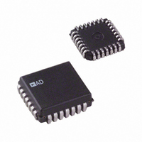
AD7846JP Analog Devices Inc, AD7846JP Datasheet - Page 13

AD7846JP
Manufacturer Part Number
AD7846JP
Description
IC DAC 16BIT LC2MOS VOUT 28PLCC
Manufacturer
Analog Devices Inc
Datasheet
1.AD7846JPZ.pdf
(24 pages)
Specifications of AD7846JP
Data Interface
Parallel
Rohs Status
RoHS non-compliant
Settling Time
7µs
Number Of Bits
16
Number Of Converters
1
Voltage Supply Source
Dual ±
Power Dissipation (max)
100mW
Operating Temperature
0°C ~ 70°C
Mounting Type
Surface Mount
Package / Case
28-LCC (J-Lead)
Resolution (bits)
16bit
Sampling Rate
143kSPS
Input Channel Type
Parallel
Supply Voltage Range - Digital
4.75V To 5.25V
Supply Current
5mA
Digital Ic Case Style
LCC
Lead Free Status / RoHS Status
Contains lead / RoHS non-compliant
Available stocks
Company
Part Number
Manufacturer
Quantity
Price
Company:
Part Number:
AD7846JP
Manufacturer:
AD
Quantity:
1 980
Company:
Part Number:
AD7846JP
Manufacturer:
AD
Quantity:
5 510
Part Number:
AD7846JP
Manufacturer:
ADI/亚德诺
Quantity:
20 000
Company:
Part Number:
AD7846JP-REEL
Manufacturer:
AD
Quantity:
5 510
Company:
Part Number:
AD7846JP-REEL
Manufacturer:
LT
Quantity:
5 510
Company:
Part Number:
AD7846JP-REEL
Manufacturer:
Analog Devices Inc
Quantity:
10 000
Company:
Part Number:
AD7846JPZ
Manufacturer:
Analog Devices Inc
Quantity:
10 000
Part Number:
AD7846JPZ
Manufacturer:
ADI/亚德诺
Quantity:
20 000
Company:
Part Number:
AD7846JPZ-REEL
Manufacturer:
Analog Devices Inc
Quantity:
10 000
UNIPOLAR BINARY OPERATION
Figure 23 shows the AD7846 in the unipolar binary circuit
configuration. The DAC is driven by the
Because R
and the output range is 0 V to +10 V. If a 0 V to +5 V range is
required, R
stage for a gain of 1. Table 8 gives the code table for the circuit
of Figure 23.
1µF
C1
8
GROUND
SIGNAL
AD586
IN
IN
2
4
is tied to 0 V, the output amplifier has a gain of 2
should be tied to V
*ADDITIONAL PINS
Figure 23. Unipolar Binary Operation
OMITTED FOR CLARITY
6
5
R1
10kΩ
7
8
V
V
REF+
REF–
OUT
+15V
V
4
DD
AD7846*
, configuring the output
–15V
V
AD586
SS
V
+5V
DGND
21
CC
V
OUT
R
+5 V reference.
IN
20
5
6
V
(0V TO +10V)
OUT
Rev. G | Page 13 of 24
Table 8. Code Table for Figure 23
Binary Number in DAC Latch
MSB
1111 1111 1111 1111
1000 0000 0000 0000
0000 0000 0000 0001
0000 0000 0000 0000
1
Offset and gain can be adjusted in Figure 23 as follows:
•
•
LSB = 10 V/2
To adjust offset, disconnect the V
the DAC with all 0s, and adjust the V
= 0 V.
For gain adjustment, the AD7846 should be loaded with all
1s and R1 adjusted until V
9.999847 V. If a simple resistor divider is used to vary the
V
coefficients of these resistors match that of the DAC input
resistance (−300 ppm/°C). Otherwise, extra offset errors are
introduced over temperature. Many circuits do not require
these offset and gain adjustments. In these circuits, R1 can
be omitted. Pin 5 of the AD586 can be left open circuit and
Pin 8 (V
REF−
voltage, it is important that the temperature
16
= 10 V/65,536 = 152 μV.
REF−
) of the AD7846 tied to 0 V.
LSB
1
OUT
Analog Output (V
+10 (65,535/65,536) V
+10 (32,768/65,536) V
+10 (1/65,536) V
0 V
= 10 (65,535)/(65,536) =
REF−
REF−
input from 0 V, load
voltage until V
AD7846
OUT
)
OUT


