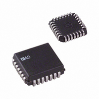
AD7846JP Analog Devices Inc, AD7846JP Datasheet - Page 18

AD7846JP
Manufacturer Part Number
AD7846JP
Description
IC DAC 16BIT LC2MOS VOUT 28PLCC
Manufacturer
Analog Devices Inc
Datasheet
1.AD7846JPZ.pdf
(24 pages)
Specifications of AD7846JP
Data Interface
Parallel
Rohs Status
RoHS non-compliant
Settling Time
7µs
Number Of Bits
16
Number Of Converters
1
Voltage Supply Source
Dual ±
Power Dissipation (max)
100mW
Operating Temperature
0°C ~ 70°C
Mounting Type
Surface Mount
Package / Case
28-LCC (J-Lead)
Resolution (bits)
16bit
Sampling Rate
143kSPS
Input Channel Type
Parallel
Supply Voltage Range - Digital
4.75V To 5.25V
Supply Current
5mA
Digital Ic Case Style
LCC
Lead Free Status / RoHS Status
Contains lead / RoHS non-compliant
Available stocks
Company
Part Number
Manufacturer
Quantity
Price
Company:
Part Number:
AD7846JP
Manufacturer:
AD
Quantity:
1 980
Company:
Part Number:
AD7846JP
Manufacturer:
AD
Quantity:
5 510
Part Number:
AD7846JP
Manufacturer:
ADI/亚德诺
Quantity:
20 000
Company:
Part Number:
AD7846JP-REEL
Manufacturer:
AD
Quantity:
5 510
Company:
Part Number:
AD7846JP-REEL
Manufacturer:
LT
Quantity:
5 510
Company:
Part Number:
AD7846JP-REEL
Manufacturer:
Analog Devices Inc
Quantity:
10 000
Company:
Part Number:
AD7846JPZ
Manufacturer:
Analog Devices Inc
Quantity:
10 000
Part Number:
AD7846JPZ
Manufacturer:
ADI/亚德诺
Quantity:
20 000
Company:
Part Number:
AD7846JPZ-REEL
Manufacturer:
Analog Devices Inc
Quantity:
10 000
AD7846
APPLICATION HINTS
NOISE
In high resolution systems, noise is often the limiting factor.
With a 10 V span, a 16-bit LSB is 152 μV (–96 dB). Thus, the
noise floor must stay below −96 dB in the frequency range of
interest. Figure 12 shows the noise spectral density for the
AD7846.
GROUNDING
As well as noise, the other prime consideration in high resolution
DAC systems is grounding. With an LSB size of 152 μV and a
load current of 5 mA, 1 LSB of error can be introduced by series
resistance of only 0.03 Ω.
Figure 30 shows recommended grounding for the AD7846 in a
typical application.
*ADDITIONAL PINS OMITTED FOR CLARITY
GROUND
SIGNAL
ANALOG SUPPLY
+15V 0V
2
AD588*
9
R1
–15V
16
15
14
1
3
Figure 30. AD7846 Grounding
R2
R3
R5
8
7
4
AD7846*
9
DIGITAL SUPPLY
+5V
21
DGND
20
6
5
R4
R
L
V
(+5V TO –5V)
OUT
Rev. G | Page 18 of 24
R1 to R5 represent lead and track resistances on the printed
circuit board. R1 is the resistance between the analog power
supply ground and the signal ground. Because current flowing
in R1 is very low (bias current of
effect of R1 is negligible. R2 and R3 represent track resistance
between the AD588 outputs and the AD7846 reference inputs.
Because of the force and sense outputs on the AD588, these
resistances will also have a negligible effect on accuracy.
R4 is the resistance between the DAC output and the load. If R
is constant, then R4 introduces a gain error only that can be
trimmed out in the calibration cycle. R5 is the resistance
between the load and the analog common. If the output voltage
is sensed across the load, R5 introduces a further gain error,
which can be trimmed out. If, on the other hand, the output
voltage is sensed at the analog supply common, R5 appears as
part of the load and therefore introduces no errors.
PRINTED CIRCUIT BOARD LAYOUT
Figure 31 shows the AD7846 in a typical application with the
AD588 reference, producing an output analog voltage in the
±10 V range. Full-scale and bipolar zero adjustment are
provided by Potentiometer R2 and Potentiometer R3. Latches
(2 × 74LS245) isolate the DAC digital inputs from the active
microprocessor bus and minimize digital feedthrough.
AD588
sense amplifier), the
L


