DAC1405D750HW/C1,5 NXP Semiconductors, DAC1405D750HW/C1,5 Datasheet
DAC1405D750HW/C1,5
Specifications of DAC1405D750HW/C1,5
Available stocks


Related parts for DAC1405D750HW/C1,5


DAC1405D750HW/C1,5 Summary of contents
Page 1
DAC1405D750 Dual 14-bit DAC 750 Msps; 4 and 8 interpolating Rev. 3 — 7 September 2010 1. General description The DAC1405D750 is a high-speed 14-bit dual channel Digital-to-Analog Converter (DAC) with selectable 4 or 8 interpolating filters optimized ...
Page 2
... NXP Semiconductors 3. Applications Wireless infrastructure: LTE, WiMAX, GSM, CDMA, WCDMA, TD-SCDMA Communication: LMDS/MMDS, point-to-point Direct Digital Synthesis (DDS) Broadband wireless systems Digital radio links Instrumentation Automated Test Equipment (ATE) 4. Ordering information Table 1. Ordering information ...
Page 3
Block diagram SDO DAC1405D750 18 to 25, FIR1 FIR2 28 to 31, 34, 35 LATCH I0 to I13 × dual port/ interleaved data modes FIR1 FIR2 41, 42, LATCH × 51 ...
Page 4
... NXP Semiconductors 6. Pinning information 6.1 Pinning 1 V DDA(3V3) 2 AUXAP AUXAN 3 AGND DDA(1V8 DDA(1V8) 7 AGND CLKP 8 CLKN 9 AGND DDA(1V8) 12 SYNCP SYNCN 13 TM1 14 TM0 DD(IO)(3V3) 17 GNDIO I13 18 I12 19 I11 20 21 I10 Fig 2. Pin configuration DAC1405D750 Product data sheet Dual 14-bit DAC 750 Msps; 4 and 8 interpolating ...
Page 5
... NXP Semiconductors 6.2 Pin description Table 2. Symbol V DDA(3V3) AUXAP AUXAN AGND V DDA(1V8) V DDA(1V8) AGND CLKP CLKN AGND V DDA(1V8) SYNCP SYNCN TM1 TM0 V DD(IO)(3V3) GNDIO I13 I12 I11 I10 DDD(1V8) DGND DDD(1V8) DGND DDD(1V8) DGND TM2 DGND DAC1405D750 Product data sheet Dual 14-bit DAC 750 Msps ...
Page 6
... NXP Semiconductors Table 2. Symbol V DDD(1V8) Q13/SELIQ Q12 DGND V DDD(1V8) Q11 Q10 Q9 Q8 DGND V DDD(1V8 GNDIO V DD(IO)(3V3) TM3 SDO SDIO SCLK SCS_N RESET_N d.n.c. VIRES GAPOUT V DDA(1V8) V DDA(1V8) AGND AUXBN AUXBP V DDA(3V3) AGND V DDA(1V8) AGND V DDA(1V8) AGND DAC1405D750 Product data sheet Dual 14-bit DAC 750 Msps ...
Page 7
... NXP Semiconductors Table 2. Symbol V DDA(1V8) AGND V DDA(1V8) AGND IOUTBN IOUTBP AGND n.c. AGND IOUTAP IOUTAN AGND V DDA(1V8) AGND V DDA(1V8) AGND V DDA(1V8) AGND V DDA(1V8) AGND AGND [ power supply G = ground I = input O = output. [ heatsink (exposed die pad to be soldered) DAC1405D750 Product data sheet Dual 14-bit DAC 750 Msps; 4 and 8 interpolating Pin description … ...
Page 8
... NXP Semiconductors 7. Limiting values Table 3. Limiting values In accordance with the Absolute Maximum Rating System (IEC 60134). Symbol Parameter V input/output supply voltage (3.3 V) DD(IO)(3V3) V analog supply voltage (3.3 V) DDA(3V3) V analog supply voltage (1.8 V) DDA(1V8) V digital supply voltage (1.8 V) DDD(1V8) V input voltage ...
Page 9
... NXP Semiconductors 9. Characteristics Table 5. Characteristics 1 DDA(1V8) DDD(1V8) DDA(3V3) +85 C; typical values measured at T amb otherwise specified. Symbol Parameter V input/output supply voltage DD(IO)(3V3) (3 analog supply voltage DDA(3V3) (3 analog supply voltage DDA(1V8) (1 digital supply voltage (1.8 V) DDD(1V8) I input/output supply current DD(IO)(3V3) (3 ...
Page 10
... NXP Semiconductors Table 5. Characteristics …continued 1 DDA(1V8) DDD(1V8) DDA(3V3) +85 C; typical values measured at T amb otherwise specified. Symbol Parameter Clock inputs (CLKP and CLKN) V input voltage i V input differential threshold idth voltage R input resistance i C input capacitance i Clock outputs (SYNCP and SYNCN) ...
Page 11
... NXP Semiconductors Table 5. Characteristics …continued 1 DDA(1V8) DDD(1V8) DDA(3V3) +85 C; typical values measured at T amb otherwise specified. Symbol Parameter Input timing (see Figure 10) f data rate data t CLK pulse width w(CLK) t input hold time h(i) t input set-up time su(i) ...
Page 12
... NXP Semiconductors Table 5. Characteristics …continued 1 DDA(1V8) DDD(1V8) DDA(3V3) +85 C; typical values measured at T amb otherwise specified. Symbol Parameter IMD3 third-order intermodulation distortion ACPR adjacent channel power ratio NSD noise spectral density [ guaranteed by design guaranteed by characterization 100 % industrially tested. ...
Page 13
... NXP Semiconductors 10. Application information 10.1 General description The DAC1405D750 is a dual 14-bit DAC which operates 750 Msps. Each DAC consists of a segmented architecture, comprising a 6-bit thermometer sub-DAC and an 8-bit binary weighted sub-DAC. The input data rate 185 MHz combined with the maximum output sampling rate of 750 Msps make the DAC1405D750 extremely flexible in wide bandwidth and multi-carrier systems. The device’ ...
Page 14
... NXP Semiconductors RESET_N SCS_N SCLK SDIO R SDO (optional) R/W indicates the mode access, (see Fig 3. SPI protocol Table 6. R Table 7 Table A4: indicate which register is being addressed. In the case of a multiple transfer, this address concerns the first register after which the next registers follow directly in a decreasing order according to 10 ...
Page 15
... NXP Semiconductors The SPI timing characteristics are given in Table 8. Symbol f SCLK t w(SCLK) t su(SCS_N) t h(SCS_N) t su(SDIO) t h(SDIO) t w(RESET_N) 10.2.3 Detailed descriptions of registers An overview of the details for all registers is provided in DAC1405D750 Product data sheet Dual 14-bit DAC 750 Msps; 4 and 8 interpolating ...
Page 16
Table 9. Register allocation map Address Register name R/W Bit definition Dec Hex Bit 7 0 00h COMMon R/W 3W_SPI 1 01h TXCFG R/W NCO_ON 2 02h PLLCFG R/W PLL_PD 3 03h FREQNCO_LSB R/W 4 04h FREQNCO_LISB R/W 5 05h ...
Page 17
... NXP Semiconductors 10.2.4 Detailed register descriptions Please refer to following tables, all the values shown in bold are the default values. Table 10. Default settings are shown highlighted. Bit Table 11. Default settings are shown highlighted. Bit Symbol 7 NCO_ON 6 NCO_LP_SEL 5 INV_SIN_SEL DAC1405D750 Product data sheet Dual 14-bit DAC 750 Msps ...
Page 18
... NXP Semiconductors Table 11. Default settings are shown highlighted. Bit Symbol MODULATION[2: INTERPOLATION[1:0] Table 12. Default settings are shown highlighted. Bit PLL_DIV[1: DAC_CLK_DELAY[1:0] R/W 0 Table 13. Bit FREQ_NCO[7:0] DAC1405D750 Product data sheet Dual 14-bit DAC 750 Msps; 4 and 8 interpolating TXCFG register (address 01h) bit description ...
Page 19
... NXP Semiconductors Table 14. Bit FREQ_NCO[15:8] Table 15. Bit FREQ_NCO[23:16] Table 16. Bit FREQ_NCO[31:24] Table 17. Bit PH_NCO[7:0] Table 18. Bit PH_NCO[15:8] Table 19. Default settings are shown highlighted. Bit DAC_A_OFFSET[5:0] Table 20. Bit DAC_A_GAIN_ DAC_A_GAIN_ DAC1405D750 Product data sheet Dual 14-bit DAC 750 Msps; 4 and 8 interpolating ...
Page 20
... NXP Semiconductors Table 21. Bit DAC_A_GAIN_ DAC_A_ Table 22. Default settings are shown highlighted. Bit DAC_B_OFFSET[5:0] Table 23. Bit DAC_B_GAIN_ DAC_B_GAIN_ Table 24. Bit DAC_B_GAIN_ DAC_B_ Table 25. Default settings are shown highlighted. Bit DAC1405D750 Product data sheet Dual 14-bit DAC 750 Msps; 4 and 8 interpolating ...
Page 21
... NXP Semiconductors Table 26. Default settings are shown highlighted. Bit Table 27. Bit AUX_A[9:2] Table 28. Default settings are shown highlighted. Bit AUX_A[1:0] Table 29. Bit AUX_B[9:2] Table 30. Default settings are shown highlighted. Bit DAC1405D750 Product data sheet Dual 14-bit DAC 750 Msps; 4 and 8 interpolating ...
Page 22
... NXP Semiconductors 10.2.5 Recommended configuration It is recommended that the following additional settings are used to obtain optimum performance 750 Msps. Table 31. Address Dec 10.3 Input data The setting applied to MODE_SEL (register 00h[3]; see whether the DAC1405D750 operates in the Dual-port mode or in Interleaved mode (see Table 32) ...
Page 23
... NXP Semiconductors Fig 6. In Interleaved mode, both DACs use the same data input at twice the Dual-port mode frequency. Data enters the latch on the rising edge of the internal clock signal. The data is sent to either latch I or latch Q, depending on the SELIQ signal. The SELIQ input (pin 41) allows the synchronization of the internally demultiplexed I and Q channels ...
Page 24
... NXP Semiconductors 10.4 Input clock The DAC1405D750 can operate at the following clock frequencies: PLL on 185 MHz in Dual-port mode and up to 370 MHz in Interleaved mode PLL off 750 MHz The input clock is LVDS compliant (see differential sine wave signal (see Fig 8. Fig 9. ...
Page 25
... NXP Semiconductors (SYNCP − SYNCN) Fig 10. Input timing diagram when internal PLL bypassed (off) 10.5.1 Timing when using the internal PLL (PLL on) In Table 33 The setting applied to PLL_DIV[1:0] (register 02h[4:3]; see map”) allows the frequency between the digital part and the DAC core to be adjusted. ...
Page 26
... NXP Semiconductors Table 36. First interpolation filter Lower H(1) H(2) H(3) H(4) H(5) H(6) H(7) H(8) H(9) H(10) H(11) H(12) H(13) H(14) H(15) H(16) H(17) H(18) H(19) H(20) H(21) H(22) H(23) H(24) H(25) H(26) H(27) H(28) 10.7 Quadrature modulator and Numerically Controlled Oscillator The quadrature modulator allows the 14-bit I and Q-data to be mixed with the carrier signal generated by the NCO ...
Page 27
... NXP Semiconductors 10.7.1 NCO in 32-bit When using the NCO, the frequency can be set by the four registers FREQNCO_LSB, FREQNCO_LISB, FREQNCO_UISB and FREQNCO_MSB over 32 bits. The frequency for the NCO in 32-bit is calculated as follows: f NCO where M is the decimal representation of FREQ_NCO[31:0]. The phase of the NCO can be set from 0 to 360 by both registers PHINCO_LSB and PHINCO_MSB over 16 bits ...
Page 28
... NXP Semiconductors 10.9 DAC transfer function The full-scale output current for each DAC is the sum of the two complementary current outputs The output current depends on the digital input data: I IOUTP I IOUTN The setting applied to CODING (register 00h[2]; see defines whether the DAC1405D750 operates with a binary input or a two’s complement input. Table 38 “ ...
Page 29
... NXP Semiconductors Fig 11. Internal reference configuration This configuration is optimum for temperature drift compensation because the bandgap reference voltage can be matched to the voltage across the feedback resistor. The DAC current can also be set by applying an external reference voltage to the non-inverting input pin GAPOUT and disabling the internal bandgap reference voltage with GAP_PD (register 00h[0] ...
Page 30
... NXP Semiconductors Table 39. Default settings are shown highlighted. DAC_GAIN_COARSE[3:0] Decimal The settings applied to DAC_A_GAIN_FINE[5:0] (see (address 0Ah) bit “DAC_B_Cfg_2 register (address 0Dh) bit full-scale current (see Table 40. Default settings are shown highlighted. DAC_GAIN_FINE[5:0] Decimal 32 ... 0 ... 31 The coding of the fine gain adjustment is two’s complement. ...
Page 31
... NXP Semiconductors Table 41. Default settings are shown highlighted. DAC_OFFSET[11:0] Decimal 2048 2047 ... ... +2046 +2047 10.12 Analog output The DAC1405D750 has two output channels each of which produces two complementary current outputs. These allow the even-order harmonics and noise to be reduced. The pins ...
Page 32
... NXP Semiconductors 10.13 Auxiliary DACs The DAC1405D750 integrates 2 auxiliary DACs that can be used to compensate for any offset between the DAC and the next stage in the transmission path. Both auxiliary DACs have a resolution of 10-bit and are current sources (referenced to ground). I O AUX ...
Page 33
... NXP Semiconductors The DAC1405D750 differential outputs can operate recommended to connect the center tap of the transformer resistor connected to the 3.3 V analog power supply, in order to adjust the DC common mode to approximately 2.7 V (see Fig 14 10.14.2 DC interface to an Analog Quadrature Modulator (AQM) When the system operation requires to keep the DC component of the spectrum, the DAC1405D750 can use a DC interface to connect to an AQM ...
Page 34
... NXP Semiconductors Fig 16. An example interface to a 3.3 V The auxiliary DACs can be used to control the offset in a precise range or with precise steps. Figure 17 a 1.7 V Fig 17. An example interface to a 1.7 V Figure 18 a 3.3 V DAC1405D750 Product data sheet Dual 14-bit DAC 750 Msps; 4 and 8 interpolating ...
Page 35
... NXP Semiconductors Fig 18. An example interface to a 3.3 V The constraints to adjust the interface are the output compliance range of the DAC and the auxiliary DACs, the input common mode level of the AQM, and the range of offset correction. 10.14.3 AC interface to an Analog Quadrature Modulator (AQM) When the AQM common mode voltage is close to ground, the DAC1405D750 must be AC-coupled and the auxiliary DACs are needed for offset correction ...
Page 36
... NXP Semiconductors Fig 19. An example interface to a 0.5 V 10.15 Power and grounding In order to obtain optimum performance recommended that the 1.8 V analog power supplies on pins 5, 11, 71, 77 and 99 should not be connected with the ones on pins 6, 70, 79, 81, 83, 93, 95 and 97 on the top layer. ...
Page 37
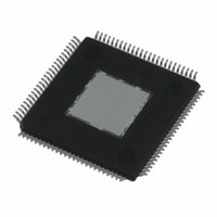
... NXP Semiconductors 11. Package outline HTQFP100: plastic thermal enhanced thin quad flat package; 100 leads; body mm; exposed die pad y exposed die pad side pin 1 index 100 DIMENSIONS (mm are the original dimensions) A UNIT max. 0.15 1.05 0.27 mm 1.2 0.25 0.05 0.95 0.17 Note 1 ...
Page 38
... NXP Semiconductors 12. Abbreviations Table 43. Acronym B CDMA CML CMOS DAC FIR GSM IF IMD3 LISB LMDS LSB LTE LVDS MMDS MSB NCO NMOS PLL SFDR SPI TD-SCDMA UISB WCDMA WiMAX DAC1405D750 Product data sheet Dual 14-bit DAC 750 Msps; 4 and 8 interpolating ...
Page 39
... NXP Semiconductors 13. Glossary Spurious-Free Dynamic Range (SFDR): — The ratio between the RMS value of the reconstructed output sine wave and the RMS value of the largest spurious observed (harmonic and non-harmonic, excluding DC component) in the frequency domain. Intermodulation Distortion (IMD): — From a dual-tone digital input sine wave (these two frequencies being close together), the intermodulation distortion products IMD2 and IMD3 (respectively, second and third-order components) are defined below ...
Page 40
... In no event shall NXP Semiconductors be liable for any indirect, incidental, punitive, special or consequential damages (including - without limitation - lost profits, lost savings, business interruption, costs related to the removal or ...
Page 41
... Dual 14-bit DAC 750 Msps; 4 and 8 interpolating NXP Semiconductors’ specifications such use shall be solely at customer’s own risk, and (c) customer fully indemnifies NXP Semiconductors for any liability, damages or failed product claims resulting from customer design and use of the product for automotive applications beyond NXP Semiconductors’ ...
Page 42
... NXP Semiconductors 17. Contents 1 General description . . . . . . . . . . . . . . . . . . . . . . 1 2 Features and benefits . . . . . . . . . . . . . . . . . . . . 1 3 Applications . . . . . . . . . . . . . . . . . . . . . . . . . . . . 2 4 Ordering information . . . . . . . . . . . . . . . . . . . . . 2 5 Block diagram . . . . . . . . . . . . . . . . . . . . . . . . . . 3 6 Pinning information . . . . . . . . . . . . . . . . . . . . . . 4 6.1 Pinning . . . . . . . . . . . . . . . . . . . . . . . . . . . . . . . 4 6.2 Pin description . . . . . . . . . . . . . . . . . . . . . . . . . 5 7 Limiting values Thermal characteristics . . . . . . . . . . . . . . . . . . 8 9 Characteristics . . . . . . . . . . . . . . . . . . . . . . . . . . 9 10 Application information 10.1 General description . . . . . . . . . . . . . . . . . . . . 13 10.2 Serial peripheral interface ...