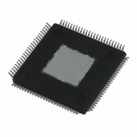
DAC1405D750HW/C1,5 NXP Semiconductors, DAC1405D750HW/C1,5 Datasheet - Page 17

DAC1405D750HW/C1,5
Manufacturer Part Number
DAC1405D750HW/C1,5
Description
IC DAC 14BIT SRL/SPI 100HTQFP
Manufacturer
NXP Semiconductors
Datasheet
1.DAC1405D750HWC15.pdf
(42 pages)
Specifications of DAC1405D750HW/C1,5
Settling Time
20ns
Number Of Bits
14
Data Interface
Serial, SPI™
Number Of Converters
2
Voltage Supply Source
Analog and Digital
Power Dissipation (max)
1.11W
Operating Temperature
-45°C ~ 85°C
Mounting Type
Surface Mount
Package / Case
100-TQFP Exposed Pad, 100-eTQFP, 100-HTQFP, 100-VQFP
Conversion Rate
750 MSPs
Resolution
14 bit
Interface Type
SPI
Supply Voltage (max)
3.6 V
Supply Voltage (min)
3 V
Maximum Operating Temperature
+ 85 C
Mounting Style
SMD/SMT
Maximum Power Dissipation
1.11 W
Minimum Operating Temperature
- 40 C
Supply Current
44 mA
Lead Free Status / RoHS Status
Lead free / RoHS Compliant
Other names
568-5089
Available stocks
Company
Part Number
Manufacturer
Quantity
Price
Company:
Part Number:
DAC1405D750HW/C1,5
Manufacturer:
IDT, Integrated Device Technology Inc
Quantity:
10 000
NXP Semiconductors
DAC1405D750
Product data sheet
10.2.4 Detailed register descriptions
Please refer to
following tables, all the values shown in bold are the default values.
Table 10.
Default settings are shown highlighted.
Table 11.
Default settings are shown highlighted.
Bit
7
6
5
4
3
2
1
0
Bit
7
6
5
Symbol
NCO_ON
NCO_LP_SEL
INV_SIN_SEL
3W_SPI
SPI_RST
-
CODING
GAP_PD
Symbol
CLK_SEL
MODE_SEL
IC_PD
COMMon register (address 00h) bit description
TXCFG register (address 01h) bit description
Table 9
All information provided in this document is subject to legal disclaimers.
Rev. 3 — 7 September 2010
for the register overview and relevant default values. In the
Dual 14-bit DAC, up to 750 Msps; 4 and 8 interpolating
R/W
R/W
R/W
R/W
Access Value Description
R/W
-
R/W
R/W
R/W
Access Value Description
R/W
R/W
0
1
0
1
0
1
-
0
1
0
1
0
1
0
1
0
1
0
1
0
1
NCO
low-power NCO
x / (sin x) function
serial interface bus type
serial interface reset
data input latch
reserved
input data mode
coding
power-down
internal bandgap power-down
disabled (the NCO phase is reset to 0)
enabled
disabled
NCO frequency and phase given by the five
MSBs of the registers 06h and 08h
respectively
disabled
enabled
4 wire SPI
3 wire SPI
no reset
performs a reset on all registers except 00h
at CLK rising edge
at CLK falling edge
dual port
interleaved
binary
two’s compliment
disabled
all circuits (digital and analog, except SPI)
are switched off
power-down disabled
internal bandgap references are switched off
DAC1405D750
© NXP B.V. 2010. All rights reserved.
17 of 42


