AD5532ABC-3 Analog Devices Inc, AD5532ABC-3 Datasheet - Page 10
AD5532ABC-3
Manufacturer Part Number
AD5532ABC-3
Description
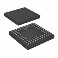
IC DAC 14BIT 32CH 74-CSPBGA
Manufacturer
Analog Devices Inc
Datasheet
1.AD5532ABCZ-1.pdf
(20 pages)
Specifications of AD5532ABC-3
Rohs Status
RoHS non-compliant
Settling Time
22µs
Number Of Bits
14
Data Interface
Serial
Number Of Converters
34
Voltage Supply Source
Analog and Digital
Power Dissipation (max)
623mW
Operating Temperature
-40°C ~ 85°C
Mounting Type
Surface Mount
Package / Case
74-CSPBGA
For Use With
EVAL-AD5532HSEBZ - BOARD EVAL FOR AD5532HSEVAL-AD5532EBZ - BOARD EVAL FOR AD5532
Available stocks
Company
Part Number
Manufacturer
Quantity
Price
Company:

Part Number:
AD5532ABC-3
Manufacturer:
AD
Quantity:
13 888
Company:
Part Number:
AD5532ABC-3
Manufacturer:
Analog Devices Inc
Quantity:
10 000


AD5532
Table 7. Pin Function Descriptions
Pin
AGND (1–2)
AV
V
V
DGND
DV
DAC_GND (1–2) Reference GND supply for all DACs.
REF_IN
REF_OUT
V
V
A4–A1, A0
CAL
CS/SYNC
WR
OFFSET_SEL
SCLK
D
D
SER/PAR
OFFS_IN
OFFS_OUT
BUSY
TRACK/RESET
DD
SS
OUT
IN
IN
OUT
CC
CC
(1–4)
(1–4)
(0–31)
(1–2)
ERROR RANGE
FULL-SCALE
VOLTAGE
OUTPUT
OFFSET
RANGE
Figure 8. DAC Transfer Function (OFFS_IN=0)
Function
Analog GND pins.
Analog Supply pins. Voltage range from 4.75 V to 5.25 V.
V
V
Digital GND pins.
Digital Supply pins. Voltage range from 2.7 V to 5.25 V.
Reference voltage for Channels 0–31.
Reference Output Voltage.
Analog Output Voltages from the 32 channels.
Analog Input Voltage. Connect this to AGND if operating in DAC mode only.
Parallel Interface: 5 address pins for 32 channels. A4 = MSB of channel address. A0 = LSB. Internal pull-up devices on these
logic inputs. Therefore, they can be left floating and default to a logic high condition.
Parallel Interface: Control input that allows all 32 channels to acquire V
these logic inputs. Therefore, they can be left floating and default to a logic low condition
This is the active low Chip Select pin for the parallel interface and the Frame Synchronization pin for the serial interface.
Parallel interface: Write pin; active low. This is used in conjunction with the CS pin to address the device using the parallel
interface. Internal pull-down devices on these logic inputs. Therefore, they can be left floating and default to a logic low
condition.
Parallel interface: Offset Select pin; active high. This is used to select the offset channel. Internal pull-down devices on
these logic inputs. Therefore, they can be left floating and default to a logic low condition
Serial Clock Input for Serial Interface. This operates at clock speeds up to 14 MHz (20 MHz in ISHA mode).
Data Input for Serial Interface. Data must be valid on the falling edge of SCLK. Internal pull-up devices on these logic
inputs. Therefore, they can be left floating and default to a logic high condition.
Output from the DAC registers for read back. Data is clocked out on the rising edge of SCLK and is valid on the falling
edge of SCLK.
This pin allows the user to select whether the serial or parallel interface is used. If the pin is tied low, the parallel interface
is used. If it is tied high, the serial interface is used. Internal pull-down devices on these logic inputs. Therefore, they can
be left floating and default to a logic low condition.
Offset Input. The user can supply a voltage here to offset the output span. OFFS_OUT can also be tied to this pin if the
user wants to drive this pin with the offset channel.
Offset Output. This is the acquired/programmed offset voltage which can be tied to OFFS_IN to offset the span.
This output tells the user when the input voltage is being acquired. It goes low during acquisition and returns high when
the acquisition operation is complete.
If this input is held high, V
stage is switched directly to V
Input section for further information. This input can also be used as a means of resetting the complete device to its
power-on-reset conditions. This is achieved by applying a low-going pulse of between 90 ns and 200 ns to this pin. See
section on RESET Function for further details. Internal pull-up devices on these logic inputs. Therefore, they can be left
floating and default to a logic high condition.
DD
SS
0
Supply pins. Voltage range from –4.75 V to –16.5 V.
Supply pins. Voltage range from 8 V to 16.5 V.
IDEAL GAIN
DAC CODE
IDEAL TRANSFER
FUNCTION
×
50mV
IDEAL GAIN
IN
is acquired once the channel is addressed. While it is held low, the input to the gain/offset
16k
IN
. The addressed channel begins to acquire V
×
REFIN
Rev. D | Page 10 of 20
V
OUT
0V
DEAD BAND
OFFSET
ERROR
LOWER
IN
simultaneously. Internal pull-down devices on
70mV
IN
on the rising edge of TRACK. See TRACK
Figure 9. ISHA Transfer Function
TRANSFER
FUNCTION
IDEAL
ACTUAL
TRANSFER
FUNCTION
DEAD BAND
2.96 3V
UPPER
GAIN ERROR +
OFFSET ERROR
V
IN
Related parts for AD5532ABC-3
Image
Part Number
Description
Manufacturer
Datasheet
Request
R

Part Number:
Description:
Cmos, 330 Mhz Triple 8-bit High Speed Video Dac
Manufacturer:
Analog Devices, Inc.
Datasheet:

Part Number:
Description:
±1.7g Dual-Axis IMEMS Accelerometer Evaluation Board
Manufacturer:
Analog Devices Inc
Datasheet:

Part Number:
Description:
Inertial Sensor Evaluation System
Manufacturer:
Analog Devices Inc
Datasheet:
Part Number:
Description:
Manufacturer:
Analog Devices Inc
Datasheet:
Part Number:
Description:
Manufacturer:
Analog Devices Inc
Datasheet:
Part Number:
Description:
Manufacturer:
Analog Devices Inc
Datasheet:
Part Number:
Description:
Manufacturer:
Analog Devices Inc
Datasheet:
Part Number:
Description:
Manufacturer:
Analog Devices Inc
Datasheet:
Part Number:
Description:
Manufacturer:
Analog Devices Inc
Datasheet:
Part Number:
Description:
Manufacturer:
Analog Devices Inc
Datasheet:
Part Number:
Description:
Manufacturer:
Analog Devices Inc
Datasheet:
Part Number:
Description:
Manufacturer:
Analog Devices Inc
Datasheet:
Part Number:
Description:
Manufacturer:
Analog Devices Inc
Datasheet: