AD5532ABC-3 Analog Devices Inc, AD5532ABC-3 Datasheet - Page 16
AD5532ABC-3
Manufacturer Part Number
AD5532ABC-3
Description
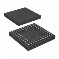
IC DAC 14BIT 32CH 74-CSPBGA
Manufacturer
Analog Devices Inc
Datasheet
1.AD5532ABCZ-1.pdf
(20 pages)
Specifications of AD5532ABC-3
Rohs Status
RoHS non-compliant
Settling Time
22µs
Number Of Bits
14
Data Interface
Serial
Number Of Converters
34
Voltage Supply Source
Analog and Digital
Power Dissipation (max)
623mW
Operating Temperature
-40°C ~ 85°C
Mounting Type
Surface Mount
Package / Case
74-CSPBGA
For Use With
EVAL-AD5532HSEBZ - BOARD EVAL FOR AD5532HSEVAL-AD5532EBZ - BOARD EVAL FOR AD5532
Available stocks
Company
Part Number
Manufacturer
Quantity
Price
Company:

Part Number:
AD5532ABC-3
Manufacturer:
AD
Quantity:
13 888
Company:
Part Number:
AD5532ABC-3
Manufacturer:
Analog Devices Inc
Quantity:
10 000


AD5532
SERIAL INTERFACE
The serial interface allows easy interfacing to most micro-
controllers and DSPs, such as the PIC16C, PIC17C, QSPI, SPI,
DSP56000, TMS320, and ADSP-21xx, without the need for any
glue logic. When interfacing to the 8051, the SCLK must be
inverted. The Microprocessor Interfacing section explains how
to interface to some popular DSPs and microcontrollers. Figure
4, Figure 5, and Figure 6 show the timing diagram for a serial
read and write to the AD5532. The serial interface works with
both a continuous and a noncontinuous serial clock. The first
falling edge of SYNC resets a counter that counts the number of
serial clocks to ensure the correct number of bits are shifted in
and out of the serial shift registers. Any further edges on SYNC
are ignored until the correct number of bits are shifted in or
out. Once the correct number of bits for the selected mode has
been shifted in or out, the SCLK is ignored. In order for another
serial transfer to take place the counter must be reset by the
falling edge of SYNC .
In readback, the first rising SCLK edge after the falling edge of
SYNC causes D
clocked out onto the D
rising edges. The D
state on the falling edge of the 14th SCLK. Data on the D
is latched in on the first SCLK falling edge after the falling edge
of the SYNC signal and on subsequent SCLK falling edges.
During read-back D
OUT
to leave its high impedance state and data is
OUT
IN
is ignored. The serial interface does
OUT
pin goes back into a high impedance
MSB
MSB
line and also on subsequent SCLK
MSB
1
1
MODE BITS
MODE BITS
0
MODE BITS
MSB
MODE BIT 1
1
0
c. INPUT SERIAL INTERFACE (ACQUIRE AND READ-BACK MODE)
0
1
MODE BITS
WRITTEN TO PART
WRITTEN TO PART
b. 24-BIT INPUT SERIAL WRITE WORD (DAC MODE)
d. INPUT SERIAL INTERFACE (READ-BACK MODE)
SERIAL WORD
SERIAL WORD
CAL
CAL
MODE BIT 2
a. 10-BIT SERIAL WRITE WORD (ISHA MODE)
10-BIT
10-BIT
CAL
0
Figure 21. Serial Interface Formats
OFFSET_SEL
OFFSET_SEL
IN
line
OFFSET_SEL
Rev. D | Page 16 of 20
CAL
TEST BIT
TEST BIT
0
OFFSET_SEL
0
TEST BIT
not shift data in or out until it receives the falling edge of the
SYNC signal.
Table 10
Pin
SER/PAR
SYNC,
D
D
Mode
Bits
Cal Bit
Offset Sel
Bit
Test Bit
A4–A0
DB13–
DB0
0
IN
OUT
A4–A0
, SCLK
A4–A0
LSB
A4–A0
LSB
TEST BIT
0
Description
This pin is tied high to enable the serial interface
and to disable the parallel interface. The serial
interface is controlled by the four pins that follow.
Standard 3-wire interface pins. The SYNC pin is
shared with the CS function of the parallel interface.
Data Out pin for reading back the contents of the
DAC registers. The data is clocked out on the rising
edge of SCLK and is valid on the falling edge of
SCLK.
The four different modes of operation are described
in the Modes of Operation section.
In DAC mode, this is a test bit. When high, it loads all
0s or all 1s to the 32 DACs simultaneously. In ISHA
mode, all 32 channels acquire V
when this bit is high. In ISHA mode, the acquisition
time is then 45 μs (typ) and accuracy may be
reduced. This bit is set low for normal use.
If this is set high, the offset channel is selected and
Bits A4–A0 are ignored.
Must be set low for correct operation of the part.
Used to address any one of the 32 channels
(A4 = MSB of address, A0 = LSB).
Used to write a 14-bit word into the addressed DAC
register. Only valid when in DAC mode.
NEXT FALLING EDGE OF SYNC
NEXT FALLING EDGE OF SYNC
(DB13 = MSB OF DAC WORD)
(DB13 = MSB OF DAC WORD)
READ FROM PART AFTER
READ FROM PART AFTER
MSB
MSB
A4–A0
14-BIT DATA
14-BIT DATA
DB13–DB0
DB13–DB0
DB13–DB0
LSB
LSB
LSB
LSB
IN
at the same time
Related parts for AD5532ABC-3
Image
Part Number
Description
Manufacturer
Datasheet
Request
R

Part Number:
Description:
Cmos, 330 Mhz Triple 8-bit High Speed Video Dac
Manufacturer:
Analog Devices, Inc.
Datasheet:

Part Number:
Description:
±1.7g Dual-Axis IMEMS Accelerometer Evaluation Board
Manufacturer:
Analog Devices Inc
Datasheet:

Part Number:
Description:
Inertial Sensor Evaluation System
Manufacturer:
Analog Devices Inc
Datasheet:
Part Number:
Description:
Manufacturer:
Analog Devices Inc
Datasheet:
Part Number:
Description:
Manufacturer:
Analog Devices Inc
Datasheet:
Part Number:
Description:
Manufacturer:
Analog Devices Inc
Datasheet:
Part Number:
Description:
Manufacturer:
Analog Devices Inc
Datasheet:
Part Number:
Description:
Manufacturer:
Analog Devices Inc
Datasheet:
Part Number:
Description:
Manufacturer:
Analog Devices Inc
Datasheet:
Part Number:
Description:
Manufacturer:
Analog Devices Inc
Datasheet:
Part Number:
Description:
Manufacturer:
Analog Devices Inc
Datasheet:
Part Number:
Description:
Manufacturer:
Analog Devices Inc
Datasheet:
Part Number:
Description:
Manufacturer:
Analog Devices Inc
Datasheet: