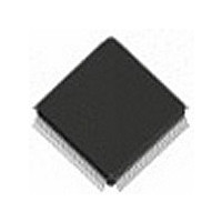
82V1068PF8 IDT, Integrated Device Technology Inc, 82V1068PF8 Datasheet - Page 8

82V1068PF8
Manufacturer Part Number
82V1068PF8
Description
Manufacturer
IDT, Integrated Device Technology Inc
Datasheet
1.82V1068PF8.pdf
(56 pages)
Specifications of 82V1068PF8
Single Supply Voltage (typ)
3.3V
Single Supply Voltage (min)
3.135V
Single Supply Voltage (max)
3.6V
Package Type
TQFP
Lead Free Status / Rohs Status
Not Compliant
IDT82V1068 OCTAL PROGRAMMABLE PCM CODEC
DX1/DU
SB1_1
SB1_2
SB1_3
SB1_4
SB1_5
SB1_6
SB1_7
SB1_8
SB2_1
SB2_2
SB2_3
SB2_4
SB2_5
SB2_6
SB2_7
SB2_8
SO1_1
SO1_2
SO1_3
SO1_4
SO1_5
SO1_6
SO1_7
SO1_8
SO2_1
SO2_2
SO2_3
SO2_4
SO2_5
SO2_6
SO2_7
SO2_8
SO3_1
SO3_2
SO3_3
SO3_4
SO3_5
SO3_6
SO3_7
SO3_8
Name
SI2_1
SI2_2
SI2_3
SI2_4
SI2_5
SI2_6
SI2_7
SI2_8
Type
I/O
I/O
O
O
O
O
I
Pin Number
101
102
128
103
127
104
126
105
125
106
10
29
37
93
74
66
30
38
94
73
65
31
39
95
72
64
32
40
96
71
63
33
41
97
70
62
34
42
98
69
61
46
2
1
9
8
7
6
5
Debounce SLIC Signaling Input 2 for Channel 1 to 8.
The input signals on these pins will be filtered by their respective debounce filters.
SLIC Signaling I/O 1 for Channel 1 to 8.
The directions of the these pins are software programmable.
SLIC Signaling I/O 2 for Channel 1 to 8.
The directions of the these pins are software programmable.
SLIC Signaling Output 1 of Channel 1 to 8.
SLIC Signaling Output 2 of Channel 1 to 8.
SLIC Signaling Output 3 of Channel 1 to 8.
DX1: Transmit PCM Data Output 1 (for MPI Mode)
In MPI mode, the DX1 pin remains in high-impedance state until a pulse appears on the FS pin. The PCM data is output
through the DX1 or DX2 pin as selected by Local Command 7, following the bit clock signal on the BCLK pin.
DU: GCI Data Upstream (for GCI Mode)
In GCI mode, the data upstream of all eight channels is sent out through the DU pin. The time slot assignment for the
eight channels is determined by the CCLK/TS pin.
8
Description
INDUSTRIAL TEMPERATURE RANGE


