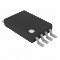
DS1851E-010+ Maxim Integrated Products, DS1851E-010+ Datasheet

DS1851E-010+
Specifications of DS1851E-010+
Related parts for DS1851E-010+
DS1851E-010+ Summary of contents
Page 1
... ORDERING INFORMATION DS1851E-010 8-pin 173mil TSSOP DS1851E-010+ 8-pin 173mil TSSOP DS1851E-010+T&R 8-pin 173mil TSSOP +Denotes a lead(Pb)-free/RoHS-compliant package. T&R = Tape and reel. DESCRIPTION The DS1851 dual temperature-controlled nonvolatile (NV) DACs consists of two DACs, two EEPROM look-up tables, and a direct-to-digital temperature sensor. Both of the DACs can be programmed with any temperature coefficient, which means that any system temperature effects can be corrected without any additional external devices ...
Page 2
DS1851 BLOCK DIAGRAM Figure 1 2-Wire SDA Interface SCL V CC GND Digital Temperature Sensor 40x8 bit 40x8 bit EEPROM EEPROM Look-Up Table 2 Look-Up Table 1 (DAC-G) (DAC-V) Table Select Byte Configuration Byte Temperature MSB Byte Temperature LSB Byte ...
Page 3
PIN DESCRIPTIONS Name Pin Description V 8 Power-Supply Terminal. The DS1851 will support supply CC voltages ranging from 3.0V to 5.5V. GND 4 Ground Terminal SDA 1 2-Wire Serial Data Interface. The serial data pin is for serial data transfer ...
Page 4
MEMORY ORGANIZATION 65h-6Fh 72h-7Fh 80h A7h F8h-FFh Table Select Byte 60h Configuration Byte 61h Temperature MSB 62h Temperature LSB 63h Address Pointer 64h User Memory DAC-V Setting 70h DAC-G Setting 71h User Memory 40x8 bit 40x8 bit EEPROM EEPROM Look-Up ...
Page 5
MEMORY LOCATIONS Memory Location Name of Location 60h Table Select Byte 61h Configuration Byte 62h Temperature MSB Function of Location Writing to this byte determines which of the two 40x8 EEPROM look-up tables is selected for reading or writing. 01h ...
Page 6
Memory Location Name of Location 63h Temperature LSB 64h Address Pointer 65h to 6Fh User Memory 70h DAC-V Setting 71h DAC-G Setting 72h to 7Fh User Memory 80h to A7h User-Defined Look-Up Table DAC OPERATION One DAC performs an 8-bit ...
Page 7
TEMPERATURE CONVERSION The direct-to-digital temperature sensor measures temperature through the use of an on-chip temperature measurement technique with an operating range from -40°C to +95°C. Temperature conversions are initiated upon power-up, and the most recent result is stored in address ...
Page 8
OPERATION Clock and Data Transitions The SDA pin is normally pulled high with an external resistor or device. Data on the SDA pin may only change during SCL low time periods. Data changes during SCL high periods will indicate ...
Page 9
Write Operations After receiving a matching address byte with the R/W bit set low, the device goes into the write mode of operation. The master must transmit an 8-bit EEPROM memory address to the device to define the address where ...
Page 10
Sequential Address Read Sequential reads are initiated by either a current address read or a random address read. After the master receives the first data byte, the master responds with an acknowledge. As long as the DS1851 receives this acknowledge ...
Page 11
Data valid: The state of the data line represents valid data when, after a START condition, the data line is stable for the duration of the HIGH period of the clock signal. The data on the line can be changed ...
Page 12
The DS1851 may operate in the following two modes: 1) Slave receiver mode: Serial data and clock are received through SDA and SCL respectively. After each byte is received, an acknowledge bit is transmitted. START and STOP conditions are recognized ...
Page 13
DATA TRANSFER PROTOCOL Figure 3 2-WIRE TIMING DIAGRAM Figure DS1851 ...
Page 14
ABSOLUTE MAXIMUM RATINGS Voltage Range on Any Pin Relative to Ground Operating Case Temperature Range Programming Temperature Range Storage Temperature Range Lead Temperature (soldering, 10s) Soldering Temperature (reflow) Lead(Pb)-free Containing Lead(Pb) *This is a stress rating only and functional operation ...
Page 15
AC ELECTRICAL CHARACTERISTICS PARAMETER SYMBOL f SCL Clock SCL Frequency t Bus Free Time BUF Between STOP and START Condition Hold Time (repeated) t HD:STA START Condition Low Period of SCL t LOW Clock High Period of SCL t HIGH ...
Page 16
DAC (-40°C to +95°C; GND + 0.1<OutG, OutV < V PARAMETER SYMBOL Resolution N Nonlinearity V INL Differential V DNL Nonlinearity Offset V off Gain Error V gain Load Regulation Output Voltage τ Time Constant and V ...
Page 17
NOTES: 1. All voltages are referenced to ground fast-mode device can be used in a standard-mode system, but the requirement t then be met. This will automatically be the case if the device does not stretch the LOW ...
Page 18
REVISION HISTORY REVISION DATE Added tape and reel part number to the Ordering Information; updated solderability information; updated Rin specifications/conditions; 1/11 added Rin temperature coefficient specification; added Package Information section DESCRIPTION DS1851 PAGES CHANGED 1, 14, 16, ...


