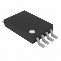
DS1851E-010+ Maxim Integrated Products, DS1851E-010+ Datasheet - Page 9

DS1851E-010+
Manufacturer Part Number
DS1851E-010+
Description
IC DAC DUAL NV TEMP CNTRL 8TSSOP
Manufacturer
Maxim Integrated Products
Datasheet
1.DS1851E-010TR.pdf
(18 pages)
Specifications of DS1851E-010+
Number Of Bits
8
Data Interface
Serial
Number Of Converters
2
Voltage Supply Source
Single Supply
Operating Temperature
-40°C ~ 95°C
Mounting Type
Surface Mount
Package / Case
8-TSSOP
Lead Free Status / RoHS Status
Lead free / RoHS Compliant
Power Dissipation (max)
-
Settling Time
-
DS1851
Write Operations
After receiving a matching address byte with the R/W bit set low, the device goes into the write mode of
operation. The master must transmit an 8-bit EEPROM memory address to the device to define the
address where the data is to be written. After the byte has been received, the DS1851 will transmit a zero
for one clock cycle to acknowledge the receipt of the address. The master must then transmit an 8-bit data
word to be written into this address. The DS1851 will again transmit a zero for one clock cycle to
acknowledge the receipt of the data. At this point, the master must terminate the write operation with a
stop condition. The DS1851 then enters an internally-timed write process T
to the EEPROM memory.
w
All inputs are disabled during this byte write cycle.
The DS1851 is capable of an 8-byte page write. A page write is initiated the same way as a byte write, but
the master does not send a STOP condition after the first byte. Instead, after the slave acknowledges
receipt of the data byte, the master can send up to seven more bytes using the same nine-clock sequence.
The master must terminate the write cycle with a STOP condition or the data clocked into the DS1851
will not be latched into permanent memory.
Acknowledge Polling
Once the internally-timed write has started and the DS1851 inputs are disabled, acknowledge polling can
be initiated. The process involves transmitting a START condition followed by the device address. The
R/W bit signifies the type of operation that is desired. The read or write sequence will only be allowed to
proceed if the internal write cycle has completed and the DS1851 responds with a zero.
Read Operations
After receiving a matching address byte with the R/W bit set high, the device goes into the read mode of
operation. There are three read operations: current address read, random read, and sequential address
read.
Current Address Read
The DS1851 has an internal address register that contains the address used during the last read or write
operation, incremented by one. This data is maintained as long as V
is valid. If the most recent address
CC
was the last byte in memory, then the register resets to the first address. This address stays valid between
operations as long as power is available.
Once the device address is clocked in and acknowledged by the DS1851 with the R/W bit set to high, the
current address data word is clocked out. The master does not respond with a zero, but does generate a
STOP condition afterwards.
Random Read
A random read requires a dummy-byte write-sequence to load in the data word address. Once the device
and data address bytes are clocked in by the master and acknowledged by the DS1851, the master must
generate another START condition. The master now initiates a current address read by sending the device
address with the R/W bit set high. The DS1851 will acknowledge the device address, then serially clocks
out the data byte.
9 of 18


