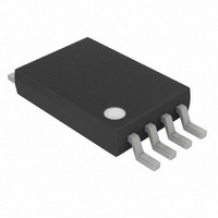
DS1851E-010+ Maxim Integrated Products, DS1851E-010+ Datasheet - Page 8

DS1851E-010+
Manufacturer Part Number
DS1851E-010+
Description
IC DAC DUAL NV TEMP CNTRL 8TSSOP
Manufacturer
Maxim Integrated Products
Datasheet
1.DS1851E-010TR.pdf
(18 pages)
Specifications of DS1851E-010+
Number Of Bits
8
Data Interface
Serial
Number Of Converters
2
Voltage Supply Source
Single Supply
Operating Temperature
-40°C ~ 95°C
Mounting Type
Surface Mount
Package / Case
8-TSSOP
Lead Free Status / RoHS Status
Lead free / RoHS Compliant
Power Dissipation (max)
-
Settling Time
-
DS1851
2-WIRE OPERATION
Clock and Data Transitions
The SDA pin is normally pulled high with an external resistor or device. Data on the SDA pin may only
change during SCL low time periods. Data changes during SCL high periods will indicate a START or
STOP conditions depending on the conditions discussed below. Refer to the Timing Diagram in Figure 4
for further details.
START Condition
A high-to-low transition of SDA with SCL high is a START condition that must precede any other
command. Refer to the timing diagram in Figure 4 for further details.
STOP Condition
A low-to-high transition of SDA with SCL high is a STOP condition. After a read sequence, the stop
command places the DS1851 into a low-power mode. Refer to the timing diagram in Figure 4 for further
details.
Acknowledge Bit
All address bytes and data bytes are transmitted via a serial protocol. The DS1851 pulls SDA low during
the ninth clock pulse to acknowledge that it has received each word.
Standby Mode
The DS1851 features a low-power mode that is automatically enabled after power-on, after a STOP
command, and after the completion of all internal operations.
2-Wire Interface Reset
After any interruption in protocol, power loss, or system reset, the following steps reset the DS1851:
1) Clock up to nine cycles.
2) Look for SDA high in each cycle while SCL is high.
3) Create a START condition while SDA is high.
Device Addressing
The DS1851 must receive an 8-bit device address word following a START condition to enable a specific
device for a read or write operation. The address word is clocked into the DS1851 MSB to LSB. The
address word consists of Ah (1010) followed by 000 then the R/W bit. If the R/W bit is high, a read
operation is initiated. The R/W is low, a write operation is initiated. Upon a match of the address, the
DS1851 will output a zero for one clock cycle as an acknowledge. If the address does not match, the
DS1851 ignores the communication.
8 of 18


