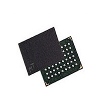
MT48H8M16LFB4-75 IT:J TR Micron Technology Inc, MT48H8M16LFB4-75 IT:J TR Datasheet - Page 52

MT48H8M16LFB4-75 IT:J TR
Manufacturer Part Number
MT48H8M16LFB4-75 IT:J TR
Description
Manufacturer
Micron Technology Inc
Type
Mobile SDRAMr
Datasheet
1.MT48H8M16LFB4-75_ITJ_TR.pdf
(75 pages)
Specifications of MT48H8M16LFB4-75 IT:J TR
Organization
8Mx16
Density
128Mb
Address Bus
14b
Access Time (max)
8/5.4ns
Maximum Clock Rate
133MHz
Operating Supply Voltage (typ)
1.8V
Package Type
VFBGA
Operating Temp Range
-40C to 85C
Operating Supply Voltage (max)
1.95V
Operating Supply Voltage (min)
1.7V
Supply Current
70mA
Pin Count
54
Mounting
Surface Mount
Operating Temperature Classification
Industrial
Lead Free Status / Rohs Status
Compliant
Figure 28:
PDF: 09005aef832ff1ea/Source: 09005aef832ff1ac
sdr_mobile_sdram_cmd_op_timing_dia_fr10_08__3.fm - Rev. E 4/09 EN
WRITE-to-WRITE
Notes:
1. DQM is LOW. Each WRITE command may be to any bank.
Data for any WRITE burst can be truncated with a subsequent READ command, and
data for a fixed-length WRITE burst can be followed immediately by a READ command.
After the READ command is registered, data input is ignored and WRITEs will not be
executed (see Figure 30 on page 53). Data n + 1 is either the last of a burst of two or the
last desired data element of a longer burst.
Data for a fixed-length WRITE burst can be followed by or truncated with a PRECHARGE
command to the same bank (provided that auto precharge was not activated), and a
continuous-page WRITE burst can be truncated with a PRECHARGE command to the
same bank. The PRECHARGE command should be issued
which the last desired input data element is registered. The auto precharge mode
requires a
In addition, when truncating a WRITE burst at high clock frequencies (
DQM signal must be used to mask input data for the clock edge prior to and the clock
edge coincident with the PRECHARGE command (see Figure 31 on page 54). Data n + 1
is either the last of a burst of two or the last desired data element of a longer burst.
Following the PRECHARGE command, a subsequent command to the same bank
cannot be issued until
In the case of a fixed-length burst being executed to completion, a PRECHARGE
command issued at the optimum time (as described above) provides the same operation
that would result from the same fixed-length burst with auto precharge. The disadvan-
tage of the PRECHARGE command is that it requires that the command and address
buses be available at the appropriate time to issue the command; the advantage of the
PRECHARGE command is that it can be used to truncate fixed-length bursts or
continuous page bursts.
Command
Address
CLK
DQ
t
WR of at least one clock with time to complete, regardless of frequency.
WRITE
Bank,
Col n
Din
T0
n
n + 1
NOP
Din
t
T1
RP is met.
128Mb: 8 Meg x 16, 4 Meg x 32 Mobile SDRAM
52
Don’t Care
WRITE
Bank,
Col b
Din
T2
b
Micron Technology, Inc., reserves the right to change products or specifications without notice.
t
WR after the clock edge at
©2008 Micron Technology, Inc. All rights reserved.
Timing Diagrams
t
CK < 15ns), the


