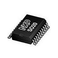
TDA8552T/N1.512 NXP Semiconductors, TDA8552T/N1.512 Datasheet - Page 11

TDA8552T/N1.512
Manufacturer Part Number
TDA8552T/N1.512
Description
Manufacturer
NXP Semiconductors
Datasheet
1.TDA8552TN1.512.pdf
(27 pages)
Specifications of TDA8552T/N1.512
Operational Class
Class-AB
Audio Amplifier Output Configuration
2-Channel Stereo
Audio Amplifier Function
Headphone/Speaker
Single Supply Voltage (typ)
5V
Dual Supply Voltage (typ)
Not RequiredV
Power Supply Requirement
Single
Power Dissipation
2.2W
Rail/rail I/o Type
No
Single Supply Voltage (min)
2.7V
Single Supply Voltage (max)
5.5V
Dual Supply Voltage (min)
Not RequiredV
Dual Supply Voltage (max)
Not RequiredV
Operating Temp Range
-40C to 85C
Operating Temperature Classification
Industrial
Mounting
Surface Mount
Pin Count
20
Lead Free Status / Rohs Status
Compliant
NXP Semiconductors
AC CHARACTERISTICS (V
T
(maximum gain = 20 dB); according to Fig.4.
Notes
1. Volume setting at maximum.
2. The noise output voltage is measured at the output in a frequency band from 20 Hz to 20 kHz (unweighted),
3. Supply voltage ripple rejection is measured at the output, with a source impedance of R
4. Channel suppression is measured at the output with a source impedance of R
2002 Jan 04
P
THD
V
SVRR
V
α
α
amb
sup
cs
o
o(n)
i(max)
2 x 1.4 W BTL audio amplifiers with digital
volume control and headphone sensing
R
The ripple voltage is a sine wave with a frequency of 1 kHz and an amplitude of 100 mV (RMS) is applied to the
positive supply rail, gain select pin is LOW (0 V).
frequency of 1 kHz. The output level in the operating single-ended channel (OUT+) is set at 2 V (RMS).
SYMBOL
= 25 °C; R
source
= 0 Ω, gain select pin is LOW (0 V).
L
= 8 Ω; f = 1 kHz; total gain setting at 7 dB; V
output power
total harmonic distortion
noise output voltage
supply voltage ripple
rejection
maximum input voltage
channel suppression
channel separation
PARAMETER
DD
= 3.3 V)
THD = 1%;
V
THD = 10%; R
THD = 10%; R
THD = 10%; R
THD = 0.5%; R
THD = 0.5%; R
THD = 0.5%; R
P
note 2
note 3
G
o
HPS
v
= 0.1 W; note 1
= −50 to 0 dB
CONDITIONS
= V
DD
11
; note 4
MODE
L
L
L
L
L
L
= 4 Ω
= 8 Ω
= 16 Ω
= 4 Ω
= 8 Ω
= 16 Ω
= 0 V; gain select pin is at 0 V
−
−
−
−
−
−
−
−
tbf
−
−
−
MIN.
TDA8552T; TDA8552TS
source
0.9
0.6
0.3
0.6
0.4
0.2
0.1
60
55
−
80
55
= 0 Ω at the input and a
TYP.
source
−
−
−
−
−
−
−
−
−
1.1
−
−
= 0 Ω at the input.
Product specification
MAX.
W
W
W
W
W
W
%
μV
dB
V
dB
dB
UNIT


