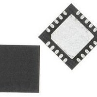
C8051F336-GMR Silicon Laboratories Inc, C8051F336-GMR Datasheet - Page 140

C8051F336-GMR
Manufacturer Part Number
C8051F336-GMR
Description
Microcontrollers (MCU) 16KB 10ADC 10DAC 768Ram MCU Lead Free
Manufacturer
Silicon Laboratories Inc
Datasheet
1.C8051F336-GM.pdf
(226 pages)
Specifications of C8051F336-GMR
Processor Series
C8051F3x
Core
8051
Data Bus Width
8 bit
Program Memory Type
Flash
Program Memory Size
16 KB
Data Ram Size
768 B
Interface Type
I2C, SPI, UART
Maximum Clock Frequency
25 MHz
Number Of Programmable I/os
17
Number Of Timers
4
Operating Supply Voltage
2.7 V to 3.6 V
Maximum Operating Temperature
+ 85 C
Mounting Style
SMD/SMT
Package / Case
QFN-20
3rd Party Development Tools
KSK-SL-TOOLSTICK, PK51, CA51, A51, ULINK2
Development Tools By Supplier
C8051F336DK
Minimum Operating Temperature
- 40 C
On-chip Adc
10 bit
On-chip Dac
10 bit
Package
20QFN
Device Core
8051
Family Name
C8051F336
Maximum Speed
25 MHz
Ram Size
768 Byte
Operating Temperature
-40 to 85 °C
Lead Free Status / Rohs Status
Details
Available stocks
Company
Part Number
Manufacturer
Quantity
Price
Company:
Part Number:
C8051F336-GMR
Manufacturer:
SILICON
Quantity:
100
Part Number:
C8051F336-GMR
Manufacturer:
SILICON LABS/èٹ¯ç§‘
Quantity:
20 000
C8051F336/7/8/9
All transactions are initiated by a master, with one or more addressed slave devices as the target. The
master generates the START condition and then transmits the slave address and direction bit. If the trans-
action is a WRITE operation from the master to the slave, the master transmits the data a byte at a time
waiting for an ACK from the slave at the end of each byte. For READ operations, the slave transmits the
data waiting for an ACK from the master at the end of each byte. At the end of the data transfer, the master
generates a STOP condition to terminate the transaction and free the bus. Figure 21.3 illustrates a typical
SMBus transaction.
21.3.1. Transmitter Vs. Receiver
On the SMBus communications interface, a device is the “transmitter” when it is sending an address or
data byte to another device on the bus. A device is a “receiver” when an address or data byte is being sent
to it from another device on the bus. The transmitter controls the SDA line during the address or data byte.
After each byte of address or data information is sent by the transmitter, the receiver sends an ACK or
NACK bit during the ACK phase of the transfer, during which time the receiver controls the SDA line.
21.3.2. Arbitration
A master may start a transfer only if the bus is free. The bus is free after a STOP condition or after the SCL
and SDA lines remain high for a specified time (see Section “21.3.5. SCL High (SMBus Free) Timeout” on
page 141). In the event that two or more devices attempt to begin a transfer at the same time, an arbitra-
tion scheme is employed to force one master to give up the bus. The master devices continue transmitting
until one attempts a HIGH while the other transmits a LOW. Since the bus is open-drain, the bus will be
pulled LOW. The master attempting the HIGH will detect a LOW SDA and lose the arbitration. The winning
master continues its transmission without interruption; the losing master becomes a slave and receives the
rest of the transfer if addressed. This arbitration scheme is non-destructive: one device always wins, and
no data is lost.
21.3.3. Clock Low Extension
SMBus provides a clock synchronization mechanism, similar to I2C, which allows devices with different
speed capabilities to coexist on the bus. A clock-low extension is used during a transfer in order to allow
slower slave devices to communicate with faster masters. The slave may temporarily hold the SCL line
LOW to extend the clock low period, effectively decreasing the serial clock frequency.
21.3.4. SCL Low Timeout
If the SCL line is held low by a slave device on the bus, no further communication is possible. Furthermore,
the master cannot force the SCL line high to correct the error condition. To solve this problem, the SMBus
protocol specifies that devices participating in a transfer must detect any clock cycle held low longer than
25 ms as a “timeout” condition. Devices that have detected the timeout condition must reset the communi-
cation no later than 10 ms after detecting the timeout condition.
140
SCL
SDA
START
SLA6
Slave Address + R/W
Figure 21.3. SMBus Transaction
SLA5-0
R/W
Rev.1.0
ACK
D7
Data Byte
D6-0
NACK
STOP


