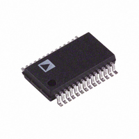
AD1955ARS Analog Devices Inc, AD1955ARS Datasheet - Page 12

AD1955ARS
Manufacturer Part Number
AD1955ARS
Description
IC DAC AUDIO MULTIBIT 28-SSOP
Manufacturer
Analog Devices Inc
Datasheet
1.AD1955ARSZ.pdf
(24 pages)
Specifications of AD1955ARS
Rohs Status
RoHS non-compliant
Number Of Bits
16, 24
Data Interface
Serial
Number Of Converters
2
Voltage Supply Source
Analog and Digital
Power Dissipation (max)
210mW
Operating Temperature
-40°C ~ 85°C
Mounting Type
Surface Mount
Package / Case
28-SSOP
For Use With
EVAL-AD1955EBZ - BOARD EVAL FOR AD1955
Settling Time
-
Available stocks
Company
Part Number
Manufacturer
Quantity
Price
Part Number:
AD1955ARSZ
Manufacturer:
ADI/亚德诺
Quantity:
20 000
AD1955
(continued from page 1)
sample rate converters. The AD1955 can be configured in left-
justified, I
modes. It can support MSB first, twos complement format, 16,
18, 20, and 24 bits in all standard PCM modes. The AD1955
also has an interface for SACD playback and an external digital
filter interface for use with an external digital interpolation filter
or HDCD decoder. The AD1955 uses a 5 V power supply. It is
fabricated on a single monolithic integrated circuit and is housed
in a 28-lead SSOP package for operation over the temperature
range –40°C to +85°C.
OPERATING FEATURES
Serial Data Input Port
The AD1955’s flexible serial data input port accepts standard
PCM audio data and external digital filter output data in twos
complement, MSB-first format in PCM/External Digital Filter
Mode, and a dedicated SACD serial port accepts DSD bit stream
data in SACD Mode. If the PCM Mode is selected by Control
Register 0 Bits 12 and 13, the left channel data field always pre-
cedes the right channel data field. The serial data format and
word length in PCM Mode are set by the mode select bits (Bits 4
and 5 and Bits 2 and 3, respectively) in the SPI control register.
In all data formats except for the Right-Justified Mode, the
serial port will accept an arbitrary number of bits up to a limit of
24 (extra bits will not cause an error, but they will be truncated
internally). In Right-Justified Mode, Control Register 0, Bits 2
and 3 are used to set the word length to 16, 18, 20, or 24 bits.
The default on power up is 24-bit, I
In the External Digital Filter Mode, selected by Control Regis-
ter 0 Bits 12 and 13, Bits 2 and 3 are used to set the word length
to 16, 18, 20, or 24 bits and the format is set with Bits 4 and 5.
For a burst-mode clock, the format should be set to left-justified.
DSP Mode is not used. The LRCLK is always falling-edge active.
The default on power-up is 24-bit mode in PCM and External
Digital Filter Mode.
In SACD Mode, selected by Control Register 0 Bits 12 and 13,
the SACD port will accept a DSD bit stream.
When the SPI Control Port is not being used, the SPI pins (24,
25, and 26) should be tied to DGND or DVDD.
TPC 31. FFT Plot, 64
0 dBFS @ 10 kHz
2
S, right-justified, or DSP serial port compatible
f
S
DSD, SR = 44.1 kHz,
2
S.
–12–
Serial Data Format in PCM Mode
The supported formats are shown in Figure 1. For detailed
timing, see Figure 2.
In Left-Justified Mode, LRCLK is high for the left channel and
low for the right channel. Data should be valid on the rising
edge of BCLK. The MSB is left-justified to an LRCLK transi-
tion, with no MSB delay.
In I
the right channel. Data should be valid on the rising edge of
BCLK. The MSB is left-justified to an LRCLK transition but
with a single BCLK period delay.
In DSP serial port mode, LRCLK must pulse high for at least
one bit clock period before the MSB of the left channel is valid,
and LRCLK must pulse high again for at least one bit clock
period before the MSB of the right channel is valid. Data should
be valid on the falling edge of BCLK. The DSP serial port mode
can be used with any word length up to 24 bits.
In this mode, it is the responsibility of the DSP to ensure that the
left data is transmitted with the first LRCLK pulse after RESET,
and that synchronism is maintained from that point forward.
In Right-Justified Mode (16 bits shown), LRCLK is high for the
left channel and low for the right channel. Data should be valid
on the rising edge of BCLK.
In normal operation, there are 64 bit clocks per frame (or 32 per
half-frame). When the SPI word length control bits (Bits 2 and
3 in Control Register 0) are set to 24 bits (0:0), the serial port
will begin to accept data starting at the eighth bit clock pulse
after the LRCLK transition. When the word length control bits
are set to 20-bit mode, data is accepted starting at the 12
clock position. In 18-bit mode, data is accepted starting at the
14
at the 16th bit clock position.
Note that the AD1955 is capable of a 32
“packed mode” where the MSB is left-justified to an LRCLK
transition, and the LSB is right-justified to the next LRCLK
transition. LRCLK is high for the left channel, and low for the
right channel. Data is valid on the rising edge of BCLK. Packed
mode can be used when the AD1955 is programmed in Left-
Justified Mode.
th
TPC 32. Wideband FFT Plot, 64
SR = 44.1 kHz, 0 dBFS @ 10 kHz
2
S Mode, LRCLK is low for the left channel and high for
bit clock position. In 16-bit mode, data is accepted starting
f
S
DSD,
f
S
BCLK frequency
REV. 0
th
bit


