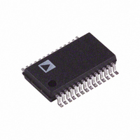
AD1955ARS Analog Devices Inc, AD1955ARS Datasheet - Page 6

AD1955ARS
Manufacturer Part Number
AD1955ARS
Description
IC DAC AUDIO MULTIBIT 28-SSOP
Manufacturer
Analog Devices Inc
Datasheet
1.AD1955ARSZ.pdf
(24 pages)
Specifications of AD1955ARS
Rohs Status
RoHS non-compliant
Number Of Bits
16, 24
Data Interface
Serial
Number Of Converters
2
Voltage Supply Source
Analog and Digital
Power Dissipation (max)
210mW
Operating Temperature
-40°C ~ 85°C
Mounting Type
Surface Mount
Package / Case
28-SSOP
For Use With
EVAL-AD1955EBZ - BOARD EVAL FOR AD1955
Settling Time
-
Available stocks
Company
Part Number
Manufacturer
Quantity
Price
Part Number:
AD1955ARSZ
Manufacturer:
ADI/亚德诺
Quantity:
20 000
AD1955
Pin No.
1
2
3
4
5
6
7
8
9
10
11
12
13
14
15
16
17
18
19
20
21
22
23
24
25
26
27
28
I/O
Input
Input
Input
Input
I/O
Input
Input
I/O
Output
Output
Output
Output
Output
Output
Output
Output
Input
Input
Input
Input
Input
Input
Mnemonic
DVDD
LRCLK/EF_WCLK
BCLK/EF_BCLK
SDATA/EF_LDATA
EF_RDATA
DSD_SCLK
DSD_LDATA
DSD_RDATA
DSD_PHASE
AGND
IOUTR+
IOUTR–
FILTR
IREF
AVDD
FILTB
IOUTL–
IOUTL+
AGND
ZEROR
ZEROL
MUTE
PD/RST
CDATA
CLATCH
CCLK
MCLK
DGND
PIN FUNCTION DESCRIPTIONS
Left/Right Clock Input for Input Data in PCM Mode
Bit Clock Input for Input Data in PCM Mode
MSB First, Twos Complement Serial Audio Data
Not used in PCM Mode
DSD Left Channel Data Input
DSD Right Channel Data Input
DSD Phase Reference Signal. This clock should be 64
Right Channel Positive Analog Output
Voltage Reference Filter Capacitor Connection. Bypass and decouple the
Left Channel Positive Analog Output
Right Channel Zero Flag Output. This pin goes high when the right channel
Left Channel Zero Flag Output. This pin goes high when the left channel has
Mute. Assert high to mute both stereo analog outputs. Deassert low for nor-
Serial Control Input, MSB First, Containing 16 Bits of Unsigned Data. Used
Master Clock Input. Connect to an external clock source.
Description
Digital Power Supply Connected to Digital 5 V Supply
Word Clock in External Filter Mode
Bit Clock Input in External Filter Mode
Two Channel (left and right), 16-Bit to 24-Bit Data in PCM Mode
Left Channel Data in External Filter Mode
Right channel data in External Filter Mode
Serial Clock Input for DSD Data. This clock should be 64
2.8224 MHz or 128
44.1 kHz, 5.6448 MHz or 256
2.8224 MHz. If not used, this pin should be connected low.
Analog Ground
Right Channel Negative Analog Output
voltage reference with parallel 10 µF and 0.1 µF capacitors to AGND.
Connection Point for External Bias Resistor
Analog Power Supply Connected to Analog 5 V Supply
Filter Capacitor Connection with Parallel 10 µF and 0.1 µF Capacitors to AGND
Left Channel Negative Analog Output
Analog Ground
has no signal input or the DSD mute pattern is detected.
no signal input or the DSD mute pattern is detected.
mal operation.
Power Down/Reset. The AD1955 is placed in a reset state and the digital
circuitry is powered down when this pin is held low. The AD1955 is reset on
the rising edge of this signal. The serial control port registers are reset to the
default values. Connect high for normal operation.
for specifying control information and channel-specific attenuation.
Latch Input for Control Data
Clock Input for Control Data. Control input data must be valid on the rising
edge of CCLK. CCLK may be continuous or gated.
Digital Ground
–6–
44.1 kHz, 5.6448 MHz in Normal Mode, 128
44.1 kHz, 11.2896 MHz in Phase Mode.
44.1 kHz,
44.1 kHz,
REV. 0


