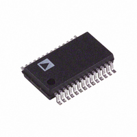
AD1955ARS Analog Devices Inc, AD1955ARS Datasheet - Page 14

AD1955ARS
Manufacturer Part Number
AD1955ARS
Description
IC DAC AUDIO MULTIBIT 28-SSOP
Manufacturer
Analog Devices Inc
Datasheet
1.AD1955ARSZ.pdf
(24 pages)
Specifications of AD1955ARS
Rohs Status
RoHS non-compliant
Number Of Bits
16, 24
Data Interface
Serial
Number Of Converters
2
Voltage Supply Source
Analog and Digital
Power Dissipation (max)
210mW
Operating Temperature
-40°C ~ 85°C
Mounting Type
Surface Mount
Package / Case
28-SSOP
For Use With
EVAL-AD1955EBZ - BOARD EVAL FOR AD1955
Settling Time
-
Available stocks
Company
Part Number
Manufacturer
Quantity
Price
Part Number:
AD1955ARSZ
Manufacturer:
ADI/亚德诺
Quantity:
20 000
AD1955
For example, with the stereo circuits given in Figures 7 through
10, this gives:
A 2.00 kΩ resistor is used.
The supply used should be as quiet as possible.
SPI REGISTER DEFINITIONS
Bit
15
14
13:12
11:10
9:8
7:6
5:4
3:2
1:0
Default = 0
[
12 0
.
V
Description
Power-Down
Mute
Data Format
Output Format
PCM Sample Rate
De-Emphasis Curve
Select
PCM/EF Serial Data
Format
PCM/EF Serial Data
Width
SPI Register Address
– .
2 80
Table I. DAC Control Register 0
V
]
[
3 24
.
mA
+
(
2 80
Value
0
1
0
1
00
01
10
11
00
01
10
11
00
01
10
11
00
01
10
11
00
01
10
11
00
01
10
11
00
.
V
2 00
.
Definition
Operation
Powered Down
Not Muted
Muted
PCM
External DF
SACD Slave
SACD Master
Stereo
Not Allowed
Mono Left
Mono Right
48 kHz
96 kHz
192 kHz
Reserved
None
44.1 kHz
32 kHz
48 kHz
I
Right-Justified
DSP
Left-Justified
24 bits
20 bits
18 bits
16 bits
2
S
K
)
]
=
1 98
.
k
Ω
–14–
Serial Control Port
The AD1955 has an SPI compatible control port to permit pro-
gramming the internal control registers. The SPI control port is
a 3-wire serial port. Its format is similar to the Motorola SPI
format except that the input data-word is 16 bits wide. The serial
bit clock may be completely asynchronous to the sample rate of the
DAC. The following figure shows the format of the SPI signal
Note that the CCLK may be continuous or a 16-clock burst.
Bit
10:9
8
7
6
5:4
3
2
1:0
Default = 0
Bit
15:2
1:0
Default = Full Volume
Description
MCLK Mode
Zero Flag Polarity
SACD Bit Rate
SACD Mode
SACD Phase Select
SACD Bit Inversion
SACD MCLK to
BCLK Phase
SPI Register Address
Description
Volume
SPI Register Address
Table III. DAC Volume Registers
Table II. DAC Control Register 1
Value
00
01
10
11
0
1
0
1
0
1
00
01
10
11
0
1
0
1
01
Value
14-Bit
Unsigned
10
11
Definition
256
512
768
Reserved
Active High
Active Low
64
128
Normal
Phase Mode
Phase 0
Phase 1
Phase 2
Phase 3
Normal
Inverted
Rising Edge
Falling Edge
Definition
Left Volume
Right Volume
f
S
f
f
f
f
S
S
S
S
REV. 0


