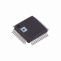
AD1953YSTRL7 Analog Devices Inc, AD1953YSTRL7 Datasheet - Page 11

AD1953YSTRL7
Manufacturer Part Number
AD1953YSTRL7
Description
IC DSP DAC AUDIO3CH/26BIT 48LQFP
Manufacturer
Analog Devices Inc
Series
SigmaDSP®r
Datasheet
1.AD1953YSTZRL.pdf
(36 pages)
Specifications of AD1953YSTRL7
Rohs Status
RoHS non-compliant
Number Of Bits
26
Data Interface
Serial
Number Of Converters
3
Voltage Supply Source
Analog and Digital
Power Dissipation (max)
540mW
Operating Temperature
-40°C ~ 105°C
Mounting Type
Surface Mount
Package / Case
48-LQFP
For Use With
EVAL-AD1953EBZ - BOARD EVAL FOR AD1953 3CH 24BIT
Settling Time
-
shifted out on the DCSOUT pin. Table XXI shows the Pro-
gram Counter Trap values and register-select values that should
be used to tap various internal points of the algorithm flow.
The DCSOUT pin is meant to be used in conjunction with the
LRCLK and BCLK signals that are provided to the serial input
port. The format of DCSOUT is the same as the format used
for the serial port. In other words, if the serial port is running in
I
and BCLK0 pins (assuming input 0 is selected), will form a
valid 3-wire I
The DCSOUT pin can be used for a variety of purposes. If the
DCSOUT pin is used to drive another external DAC, then a 4.1
system is possible using a new program downloaded into the
program RAM.
AUXDATA—Auxiliary Serial Data Input.
The AUXDATA pin may be used in conjunction with a custom
program to access two extra channels of serial input data, allow-
ing for a total of four input channels. The serial format is identical
to the selected format of SDATA0, 1, 2. The AUXDATA pin is
synchronous to the selected LRCLK and BCLK signal, and there-
fore should have the same timing as the main serial input signal.
MUTE—Mute Output Signal.
When this pin is asserted HIGH, a ramp sequence is started that
gradually reduces the volume to zero. When deasserted, the
volume ramps from zero back to the original volume setting.
The ramp speed is timed so that it takes 10 ms to reach zero
volume when starting from the default 0 dB volume setting.
VOUTL+, VOUTL– —Left-Channel Differential Analog Out-
puts. Full-scale outputs correspond to 1 V rms on each output pin,
or 2 V rms differential, assuming a VREF input voltage of 2.5 V. The
full-scale swing scales directly with VREF. These outputs are
capable of driving a load of > 5 kΩ, with a maximum peak current
of 1 mA from each pin. An external third-order filter is recom-
mended for filtering out-of-band noise.
VOUTR+, VOUTR– —Right Channel Differential Outputs.
Output characteristics are the same as for VOUTL+ and VOUTL–.
REV. 0
2
S mode, then the DCSOUT pin, together with the LRCLK0
2
S output.
–11–
VOUTS+, VOUTS– —Sub Channel Differential Outputs.
These outputs are designed to drive loads of 10 kΩ or greater,
with a peak current capability of 250 µA. This output does not
use digital interpolation, as it is intended for low frequency
application. An external third-order filter with a cutoff frequency
< 2 kHz is recommended.
VREF—Analog Reference Voltage Input.
The nominal VREF input voltage is 2.5 V; the analog gain
scales directly with the voltage on this pin. When using the
AD1953 to drive a power amplifier, it is recommended that the
VREF voltage be derived by dividing down and heavily filtering
the supply to the power amplifier. This provides a benefit if the
compressor/limiter in the AD1953 is used to prevent amplifier
clipping. In this case, if the DAC output voltage is scaled to the
amplifier power supply, a fixed compressor threshold can be
used to protect an amplifier whose supply may vary over a wide
range. Any ac signal on this pin will cause distortion, and a large
decoupling capacitor may therefore be necessary to ensure that
the voltage on VREF is clean. The input impedance of VREF is
greater than 1 MΩ.
FILTCAP—Filter Capacitor Point.
This pin is used to reduce the noise on an internal biasing point
in order to provide the highest performance. It may not be nec-
essary to connect this pin, depending on the quality of the layout
and grounding used in the application circuit.
DVDD—Digital VDD for Core.
5 V nominal.
ODVDD—Digital VDD for All Digital Outputs.
Variable from 2.7 V to 5.5 V.
DGND (2)—Digital Ground.
AVDD (3)—Analog VDD.
5 V nominal. For best results, use a separate regulator for AVDD.
Bypass capacitors should be placed close to the pins and con-
nected directly to the analog ground plane.
AGND (3)—Analog Ground.
For best performance, separate nonoverlapping analog and
digital ground planes should be used.
AD1953


