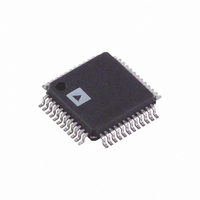
AD1953YSTRL7 Analog Devices Inc, AD1953YSTRL7 Datasheet - Page 22

AD1953YSTRL7
Manufacturer Part Number
AD1953YSTRL7
Description
IC DSP DAC AUDIO3CH/26BIT 48LQFP
Manufacturer
Analog Devices Inc
Series
SigmaDSP®r
Datasheet
1.AD1953YSTZRL.pdf
(36 pages)
Specifications of AD1953YSTRL7
Rohs Status
RoHS non-compliant
Number Of Bits
26
Data Interface
Serial
Number Of Converters
3
Voltage Supply Source
Analog and Digital
Power Dissipation (max)
540mW
Operating Temperature
-40°C ~ 105°C
Mounting Type
Surface Mount
Package / Case
48-LQFP
For Use With
EVAL-AD1953EBZ - BOARD EVAL FOR AD1953 3CH 24BIT
Settling Time
-
AD1953
Register Bits
1
0
Bit 0 is asserted when all requested safeload registers have been
transferred to the parameter RAM. It is cleared after the read
operation is complete.
Bit 1 is asserted after the requested shutdown of the DSP is
completed. When this bit is set, the user is free to write or read
any RAM location without causing an audio pop or click.
Register Bits
9
8
7:6
5:4
3
2
1:0
Table IV. Control Register 1 READ Definition
Table V. Control Register 2 WRITE Definition
Function
DSP Core Shutdown Complete
1 = Shutdown Complete
0 = Not Shut Down
Safe Memory Load Complete
1 = Complete (Note: Cleared after Read)
0 = Not Complete
Function
Volume Ramp Speed
1 = 160 ms Full-Ramp Time
0 = 20 ms Full-Ramp Time
Serial Port Output Enable
1 = Enabled
0 = Disabled
Serial Port Input Select
00 = IN0
01 = IN1
10 = IN2
11 = NA
MCLK Input Select
00 = MCLK0
01 = MCLK1
10 = MCLK2
11 = NA
Reserved
MCLK In Frequency Select
0 = 512 × f
1 = 256 × f
MCLK Out Frequency Select
00 Disabled
01 512 × f
10 256 × f
11 MCLKO = MCLK_In (Feedthrough)
S
S
S
S
–22–
Control Register 2
Table V documents the contents of Control Register 2. Bits
<1:0> set the frequency of the MCLKO pin. If these bits are set
to 00, the MCLKO pin is disabled (default). When set to 01,
the MCLKO pin is set to 512 × f
internal master clock used by the DSP core. When set to 10,
this pin is set to 256 × f
clock by 2. In this mode, the output 256 × f
with respect to the input 256 × f
the feedthrough mode. When set to 11, the MCLKO pin mirrors
the selected MCLK input pin (it’s the output of the MCLK
MUX selector). Note that the internal DSP master clock may
either be the same as the selected MCLK pin (when MCLK
frequency select is set to 512 × f
the MCLK pin using internal clock doubler (when MCLK fre-
quency select is set to 256 × f
Bit <2> selects one of two possible MCLK input frequencies. When
set to 0 (default), the MCLK frequency is set to 512 × f
the internal DSP clock and the external MCLK are at the same
frequency. When set to 1, the MCLK frequency is set to 256 × f
an internal clock doubler is used to generate the DSP clock.
Bits <5:4> select one of three clock input sources using an inter-
nal MUX. To avoid click and pop noises when switching MCLK
sources, it is recommended that the user put the DSP core in
shutdown before switching MCLK sources.
Bits <7:6> select one of three serial input sources using an inter-
nal MUX. Each source selection includes a separate SDATA,
LRCLK, and BCLK input. To avoid click and pop noises when
switching serial sources, it is recommended that the user put the
DSP core in shutdown before writing to these bits.
Bit <8> is used to enable the three serial output pins. These pins
are connected to the output of the serial input MUX, which is set
by Bits <7:6>. The default is 0 (disabled).
Bit <9> changes the default setting of the volume ramp speed.
When set to 0, it will take 1024 LRCLK periods to go from full
volume (6 dB) to infinite attention. When set to 1, the same
operation will take 8192 LRCLK periods.
S
, derived by dividing the internal DSP
S
)
.
S
S
S
mode) or may be derived from
clock. This is not the case with
, which is the same as the
S
clock will be inverted
S
. In this mode,
REV. 0
S
, and


