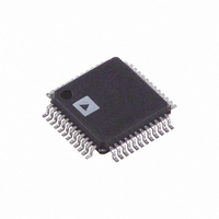
AD1953YSTRL7 Analog Devices Inc, AD1953YSTRL7 Datasheet - Page 19

AD1953YSTRL7
Manufacturer Part Number
AD1953YSTRL7
Description
IC DSP DAC AUDIO3CH/26BIT 48LQFP
Manufacturer
Analog Devices Inc
Series
SigmaDSP®r
Datasheet
1.AD1953YSTZRL.pdf
(36 pages)
Specifications of AD1953YSTRL7
Rohs Status
RoHS non-compliant
Number Of Bits
26
Data Interface
Serial
Number Of Converters
3
Voltage Supply Source
Analog and Digital
Power Dissipation (max)
540mW
Operating Temperature
-40°C ~ 105°C
Mounting Type
Surface Mount
Package / Case
48-LQFP
For Use With
EVAL-AD1953EBZ - BOARD EVAL FOR AD1953 3CH 24BIT
Settling Time
-
The detailed data format diagram for continuous-mode opera-
tion is given in SPI Read/Write data formats.
A sample timing diagram for a single SPI WRITE operation to
the parameter RAM is shown in Figure 16.
Byte 0
00000, R/Wb, adr[9:8] Adr[7:0]
A sample timing diagram of a single SPI READ operation is
shown in Figure 17. The COUT pin goes from three-state to
driven at the beginning of Byte 2. Bytes 0 and 1 contain the
address and R/W bit, and Bytes 2 to 4 carry the data. The exact
format is shown in Tables VIII to XIX.
The AD1953 has several mechanisms for updating signal-
processing parameters in real time without causing loud pops or
REV. 0
CLATCH
CDATA
CCLK
CLATCH
CDATA
Table I. SPI Word Format
CCLK
COUT
Byte 1
Figure 16. Sample of SPI WRITE Format (Single-Write Mode)
BYTE 0
Figure 17. Sample of SPI READ Format (Single-Read Mode)
Byte 2 Byte 3 Byte 4
Data
HI-Z
BYTE 0
Data
BYTE 1
Data
–19–
DATA
clicks. In cases where large blocks of data need to be downloaded,
the DSP core can be shut down and new data loaded, and the
core can then be restarted. The shutdown and restart mecha-
nisms employ a gradual volume ramp to prevent clicks and pops.
In cases where only a few parameters need to be changed (for
example, a single biquad filter), a safeload mechanism is used
that allows a block of SPI registers to be transferred to the
parameter RAM within a single audio frame while the core is
running. The safeload mode uses internal logic to prevent con-
tention between the DSP core and the SPI port.
SPI Address Decoding
Table II shows the address decoding used in the SPI port. The
SPI address space encompasses a set of registers and two RAMs,
one for holding signal-processing parameters and one for holding
the program instructions. Both of the RAMs are loaded on
power-up from on-board boot ROMs.
BYTE 1
DATA
XXX
DATA
BYTE 4
HI-Z
AD1953


