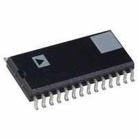
ADMCF341BR Analog Devices Inc, ADMCF341BR Datasheet - Page 22

ADMCF341BR
Manufacturer Part Number
ADMCF341BR
Description
IC DSP 3CH 12BIT MOT-CTRL 28SOIC
Manufacturer
Analog Devices Inc
Series
Motor Controlr
Type
Motor Controlr
Datasheet
1.ADMCF341BR.pdf
(36 pages)
Specifications of ADMCF341BR
Rohs Status
RoHS non-compliant
Interface
Synchronous Serial Port (SSP)
Clock Rate
20MHz
Non-volatile Memory
FLASH (12 kB), ROM (12kB)
On-chip Ram
2.5kB
Voltage - I/o
5.00V
Voltage - Core
5.00V
Operating Temperature
-40°C ~ 85°C
Mounting Type
Surface Mount
Package / Case
28-SOIC (7.5mm Width)
Available stocks
Company
Part Number
Manufacturer
Quantity
Price
Part Number:
ADMCF341BRZ
Manufacturer:
ADI/亚德诺
Quantity:
20 000
PORTA Pin
PORTA8
PORTA7
PORTA6
PORTA5
PORTA4
PORTA3
PORTA2
PORTA1
PORTA0
alternate function of PORTA7 is selected by Bit 14 of the
PORTA_SELECT register. The second alternate function of
PORTA8 is selected by Bit 15 of the PORTA_SELECT register.
The second alternate function of the PORTA4 and PORTA5
pins is selected by Bit 4 of MODECTRL Register (SPORT1
mode: boot mode/UART mode).
Once PIO functionality has been selected for any or all of these
nine pins, the direction may be set by the 9-bit PORTA_DIR
register. Clearing any bit configures the corresponding PIO line
as an input, while setting the bit configures it as an output. By
default, following a reset, all bits of PORTA_DIR are cleared,
configuring the PIO lines as inputs. The data of the PORTA0 to
PORTA8 lines is controlled by the PORTA_DATA register.
These registers can be used to read data from those PIO lines
configured as inputs and write data to those configured as outputs.
Any of the nine pins that have been configured for PIO func-
tionality can be made to act as an interrupt source by setting the
appropriate bit of the PORTA_INTEN register. To act as an
interrupt source, the pin must also be configured as an input.
An interrupt is generated upon a change of state (low-to-high
transition or high-to-low transition) on any input that has been
configured as an interrupt source. Following a change of state
event on any such input, the corresponding bit is set in the
PORTA_FLAG, register and a common PIO interrupt is generated.
Reading the PORTA_FLAG register permits determining
the interrupt source. Reading the PORTA_FLAG register
automatically clears all bits of the registers. Following power-
on or reset, all bits of PORTA_INTEN are cleared so that no
interrupts are enabled.
Each PIO line has an internal pull-down resistor so that following
power-on or reset, all nine lines are configured as input PIOs
and will be read as logic lows if left unconnected.
PIO Registers
The configuration of all registers of the PIO system is shown in
Figure 25.
INTERRUPT CONTROL
The ADMC(F)341 can respond to 18 different interrupt sources
with minimal overhead. Seven of these interrupts are internal
ADMC(F)341
AUX0 (Auxiliary PWM Output)
AUX1 (Auxiliary PWM Output)
DR1 (Data Receive SPORT1)
FL1 (Flag Out SPORT1)
SCLK1 (Serial Clock SPORT1)
TFS0 (Transmit Frame Sync SPORT0)
RFS0 (Receive Frame Sync SPORT0)
DT0 (Data Transmit SPORT0)
DR0 (Data Receive SPORT0)
First Alternate Function (Peripheral)
Table IX. Port A Multiplexing
–22–
DSP core interrupts and 11 are from the on-chip peripherals.
The seven DSP core interrupts are SPORT0 receive and
transmit, SPORT1 receive (or IRQ0) and transmit (or IRQ1),
the internal timer, and two software interrupts. The motor
control interrupts are the nine PORTA PIOs and two from the
PWM block (PWMSYNC pulse and PWMTRIP). All the on-chip
peripheral interrupts are multiplexed into the DSP core via the
peripheral IRQ2 interrupt. They are also internally prioritized
and individually maskable. The start address in the interrupt
vector table for the ADMC(F)341 interrupt sources is shown in
Table X. The interrupts are listed from highest to lowest prior-
ity. The PWMSYNC interrupt is triggered by a low-to-high
transition on the PWMSYNC pulse. The PWMTRIP interrupt
is triggered on a high-to-low transition on the PWMTRIP pin.
A PIO interrupt is detected on any change of state (high-to-low
or low-to-high) on the PIO lines.
The entire interrupt control system of the ADMC(F)341 is
configured and controlled by the IFC, IMASK, and ICNTL
registers of the DSP core, the IRQFLAG register for the
PWMSYNC and PWMTRIP interrupts, and PORTA_FLAG
register for the PIO interrupts.
Interrupt Source
PWMTRIP
Peripheral Interrupt (IRQ2)
PWMSYNC
PIO
Software Interrupt 1
Software Interrupt 0
SPORT0 Transmit Interrupt
SPORT0 Receive Interrupt
SPORT1 Transmit Interrupt (or IRQ1) 0x0020
SPORT1 Receive Interrupt (or IRQ0)
Timer
Interrupt Masking
Interrupt masking (or disabling) is controlled by the IMASK
register of the DSP core. This register contains individual bits
that must be set to enable the various interrupt sources. If any
peripheral interrupt is to be enabled, the IRQ2 interrupt enable
bit (Bit 9) of the IMASK register must be set. The configuration
of the IMASK register of the ADMC(F)341 is shown in Figure 30.
Table X. Interrupt Vector Addresses
Second Alternate Function (Peripheral)
CLKOUT (System CLOCK)
PWMSYNC (PWM)
None
DT1 (Data Transmit SPORT1)
SCLK0 (Serial Clock SPORT0)
None
None
None
None
Interrupt Vector Address
0x002C (Highest Priority)
0x0004
0x000C
0x0008
0x0018
0x001C
0x0010
0x0014
0x0024
0x0028 (Lowest Priority)
REV. B


